SSF3056C Overview
Description
It utilizes the latest trench processing techniques to achieve the high cell density and reduces the on-resistance with high repetitive avalanche rating. These features combine to make this design an extremely efficient and reliable device for use in buck-boost circuit, DSC, portable devices and a wide variety of others applications Absolute max Rating: Symbol Parameter ID @ TC = 25°C ID @ TC = 100°C IDM PD @TC = 25°C VDS VGS TJ TSTG Continuous Drain Current, VGS @ 4.5V① Continuous Drain Current, VGS @ 4.5V① Pulsed Drain Current② Power Dissipation③ Drain-Source Voltage Gate-to-Source Voltage Operating Junction and Storage Temperature Range Max.
Key Features
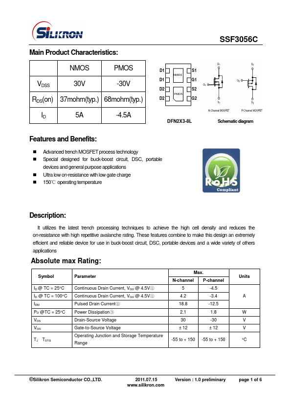
- 4.5A DFN2X3-8L Bottom View
- Advanced trench MOSFET process technology
- Special designed for buck-boost circuit, DSC, portable devices and general purpose applications
- Ultra low on-resistance with low gate charge
- 150℃ operating temperature SSF3056C