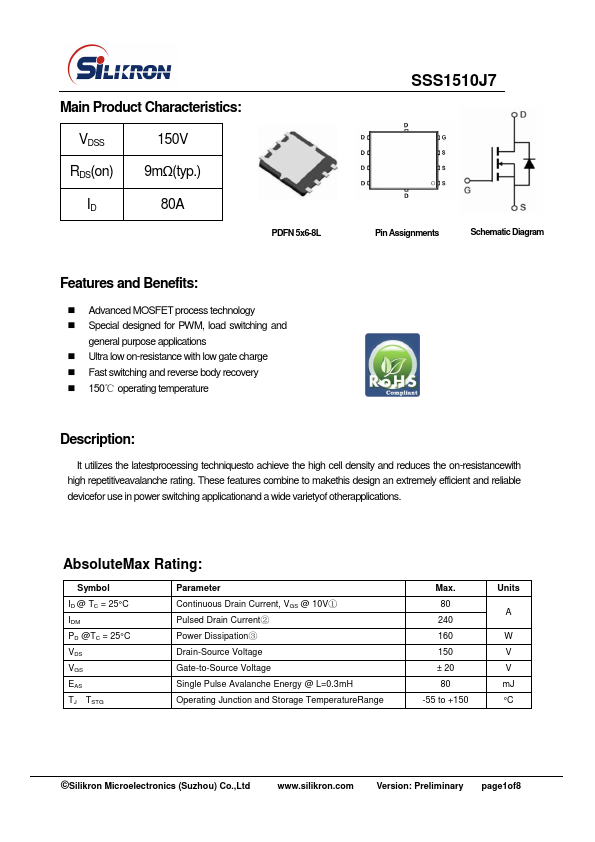
SSS1510J7
SSS1510J7 is MOSFET manufactured by Silikron.
Features and Benefits:
- Advanced MOSFET process technology
- Special designed for PWM, load switching and general purpose applications
- Ultra low on-resistance with low gate charge
- Fast switching and reverse body recovery
- 150℃ operating temperature
Description
:
It utilizes the latestprocessing techniquesto achieve the high cell density and reduces the on-resistancewith high repetitiveavalanche rating. These features bine to makethis design an extremely efficient and reliable devicefor use in power switching applicationand a wide varietyof otherapplications.
Absolute Max Rating:
Symbol ID @ TC = 25°C IDM PD @TC = 25°C VDS VGS EAS TJ TSTG
Parameter Continuous Drain Current, VGS @ 10V① Pulsed Drain Current② Power Dissipation③ Drain-Source Voltage Gate-to-Source Voltage Single Pulse Avalanche Energy @ L=0.3m H Operating Junction and Storage Temperature Range
Max. 80 240 160 150 ± 20 80
-55 to +150
Units
W V V m J °C
©Silikron Microelectronics (Suzhou) Co.,Ltd
.silikron. Version: Preliminary page1of8
Thermal Resistance
Symbol RθJC
Characterizes Junction-to-case③
Typ.
- Max. 0.78
Units ℃/W
Electrical Characterizes@TA=25℃unless otherwise specified
Symbol V(BR)DSS RDS(on) VGS(th) IDSS
IGSS
Qg Qgs Qgd td(on) tr td(off) tf Ciss Coss Crss
Parameter Drain-to-Source breakdown voltage Static Drain-to-Source on-resistance Gate threshold voltage Drain-to-Source leakage current
Gate-to-Source forward leakage
Total gate charge Gate-to-Source charge Gate-to-Drain("Miller") charge Turn-on delay time Rise time Turn-Off delay time Fall time Input capacitance Output capacitance Reverse transfercapacitance
Min. 150
- 3
- -
- -
- -
- -
- -
- -...