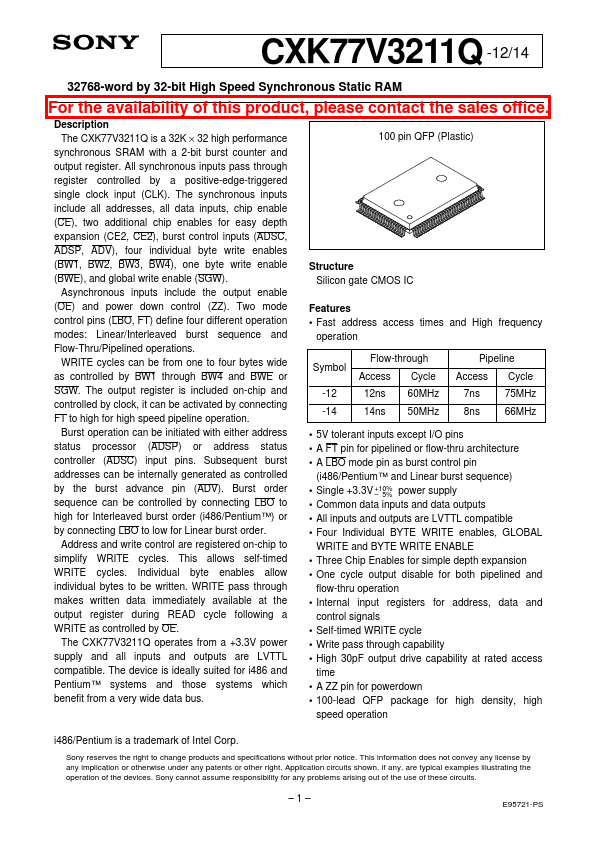
CXK77V3211Q-12
CXK77V3211Q-12 is 32768-word by 32-bit High Speed Synchronous Static RAM manufactured by Sony Semiconductor Solutions.
CXK77V3211Q -12/14
32768-word by 32-bit High Speed Synchronous Static RAM
For the availability of this product, please contact the sales office.
Description The CXK77V3211Q is a 32K × 32 high performance synchronous SRAM with a 2-bit burst counter and output register. All synchronous inputs pass through register controlled by a positive-edge-triggered single clock input (CLK). The synchronous inputs include all addresses, all data inputs, chip enable (CE), two additional chip enables for easy depth expansion (CE2, CE2), burst control inputs (ADSC, ADSP, ADV), four individual byte write enables (BW1, BW2, BW3, BW4), one byte write enable (BWE), and global write enable (SGW). Asynchronous inputs include the output enable (OE) and power down control (ZZ). Two mode control pins (LBO, FT) define four different operation modes: Linear/Interleaved burst sequence and Flow-Thru/Pipelined operations. WRITE cycles can be from one to four bytes wide as controlled by BW1 through BW4 and BWE or SGW. The output register is included on-chip and controlled by clock, it can be activated by connecting FT to high for high speed pipeline operation. Burst operation can be initiated with either address status processor (ADSP) or address status controller (ADSC) input pins. Subsequent burst addresses can be internally generated as controlled by the burst advance pin (ADV). Burst order sequence can be controlled by connecting LBO to high for Interleaved burst order (i486/Pentium™) or by connecting LBO to low for Linear burst order. Address and write control are registered on-chip to simplify WRITE cycles. This allows self-timed WRITE cycles. Individual byte enables allow individual bytes to be written. WRITE pass through makes written data immediately available at the output register during READ cycle following a WRITE as controlled by OE. The CXK77V3211Q operates from a +3.3V power supply and all inputs and outputs are LVTTL patible. The device is ideally suited for i486 and Pentium™...


