Datasheet Summary
Dual N-Channel Enhancement Mode MOSFET
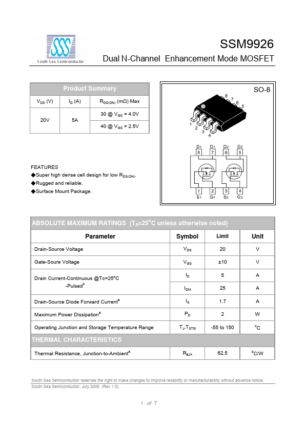
Product Summary
VDS (V) ID (A) RDS(ON) (mΩ) Max 30 @ VGS = 4.0V 20V 5A 40 @ VGS = 2.5V
SO-8
Features
- Super high dense cell design for low RDS(ON).
- Rugged and reliable.
- Surface Mount...
| Manufacturer | Part Number | Description |
|---|---|---|
| SSM9926EM | N-channel Enhancement-mode Power MOSFET | |
| SSM9926GEO | N-CHANNEL ENHANCEMENT MODE POWER MOSFET | |
| SSM9926GM | Dual N-channel Enhancement-mode Power MOSFET | |
| ETC Unknown Manufacturer |
SSM9926M | DUAL N CHANNEL ENHANCEMENT MODE POWER MOSFETS |
| SSM9926O | N-CHANNEL ENHANCEMENT MODE POWER MOSFET |