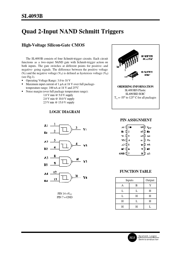
• Part: SL4093B
  • Description: Quad 2-Input NAND Schmitt Triggers
  • Manufacturer: System Logic Semiconductor
  • Size: 37.61 KB
Download SL4093B Datasheet PDF
System Logic Semiconductor
SL4093B
SL4093B is Quad 2-Input NAND Schmitt Triggers manufactured by System Logic Semiconductor.
Quad 2-Input NAND Schmitt Triggers High-Voltage Silicon-Gate CMOS The SL4093B consists of four Schmitt-trigger circuits. Each circuit functions as a two-input NAND gate with Schmitt-trigger action on both inputs. The gate switches at different points for positive- and negative- going signals. The difference between the positive voltage (VP ) and the negative voltage (VN) is defined as hysteresis voltage (VH) (see Fig.1). - Operating Voltage Range: 3.0 to 18 V - Maximum input current of 1 µA at 18 V over full packagetemperature range; 100 n A at 18 V and 25°C - Noise margin (over full package temperature range): 1.0 V min @ 5.0 V supply 2.0 V min @ 10.0 V supply 2.5 V min @ 15.0 V supply ORDERING INFORMATION SL4093BN Plastic SL4093BD SOIC TA = -55° to 125° C for all packages LOGIC DIAGRAM PIN ASSIGNMENT FUNCTION TABLE Inputs A L PIN 14 =VCC PIN 7 = GND L H H B L H L H Output Y H H H L System Logic Semiconductor MAXIMUM RATINGS - Symbol VCC VIN VOUT IIN PD PD Tstg TL - Parameter DC Supply Voltage (Referenced to GND) DC Input Voltage (Referenced to GND) DC Output Voltage (Referenced to GND) DC Input Current, per Pin Power Dissipation in Still Air, Plastic DIP+ SOIC Package+ Power Dissipation per Output Transistor Storage Temperature Lead Temperature, 1 mm from Case for 10 Seconds (Plastic DIP or SOIC Package) Value -0.5 to +20 -0.5 to VCC +0.5 -0.5 to VCC +0.5 ±10 750 500 100 -65 to +150 260 Unit V V V m A m W m W °C °C Maximum Ratings are those values beyond which damage to the device may occur. Functional operation should be restricted to the Remended Operating Conditions. +Derating - Plastic DIP: - 10 m W/°C from 65° to 125°C SOIC Package: : - 7 m W/°C from 65° to 125°C REMENDED OPERATING CONDITIONS Symbol VCC VIN, VOUT TA Parameter DC Supply Voltage (Referenced to GND) DC Input Voltage, Output Voltage (Referenced to GND) Operating Temperature, All Package Types Min 3.0 0 -55 Max 18 VCC +125 Unit V V °C This device contains...