SI9947DY
SI9947DY is Dual P-Channel Enhancement-Mode MOSFET manufactured by TEMIC Semiconductors.
Dual P-Channel Enhancement-Mode MOSFET
Product Summary
VDS (V) r DS(on) (W)
ID (A)
0.10 @ VGS =
- 10 V
"3.5
- 20
0.19 @ VGS =
- 4.5 V
"2.5
Remended upgrade: Si4947DY or Si4953DY Lower profile/smaller size- see LITE FOOTR equivalent: Si6955DQ
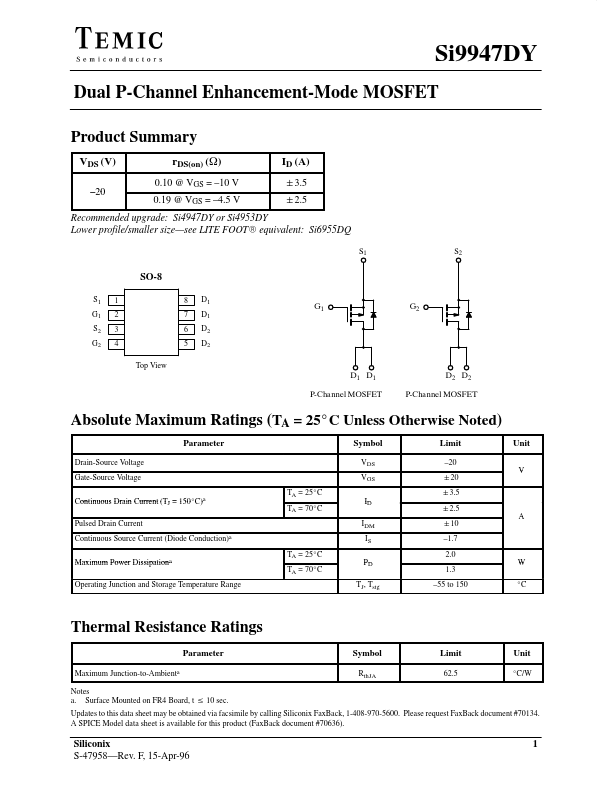
S1
S2
SO-8
S1 1 G1 2 S2 3 G2 4
Top View
8 D1 7 D1 6 D2 5 D2
G1 G2
D1 D1 PĆChannel MOSFET
D2 D2 PĆChannel MOSFET
Absolute Maximum Ratings (TA = 25_C Unless Otherwise Noted)
Parameter
Symbol
Limit
Unit
Drain-Source Voltage Gate-Source Voltage
Continuous Drain Current (TJ = 150_C)a Pulsed Drain Current Continuous Source Current (Diode Conduction)a
Maximum Power Dissipationa
Operating Junction and Storage Temperature Range
TA = 25_C TA = 70_C
TA = 25_C TA = 70_C
VDS VGS
ID IDM IS
PD TJ, Tstg
- 20 "20 "3.5 "2.5 "10
- 1.7 2.0 1.3
- 55 to...