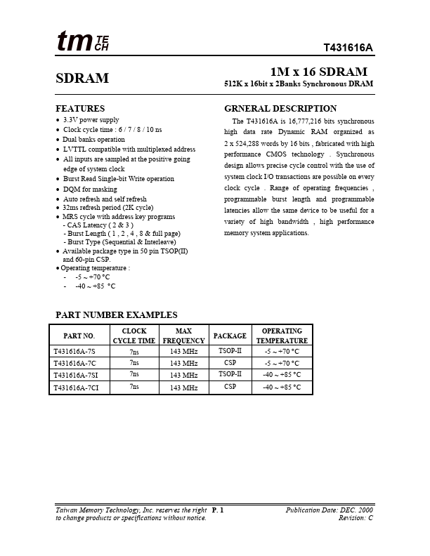
| Part | T431616A |
|---|---|
| Description | 1M x 16 SDRAM |
| Manufacturer | TM |
| Size | 1.57 MB |
Related Datasheets
| Part Number | Manufacturer | Description |
|---|---|---|
| T431616B | TMT | 1M x 16 SDRAM 512K x 16bit x 2Banks Synchronous DRAM |
| T431616C | TMT | 1M x 16 SDRAM 512K x 16bit x 2Banks Synchronous DRAM |
| T431616D | TMT | 1M x 16 SDRAM 512K x 16bit x 2Banks Synchronous DRAM |
| T431616E | TMT | 1M x 16 SDRAM 512K x 16bit x 2Banks Synchronous DRAM |
