SI2309
SI2309 is N-Channel MOSFET manufactured by TRR.
Features
- VDS (V) =-60V
- ID =-1.25 A (VGS =-10V)
- RDS(ON) < 340mΩ (VGS =-10V)
- RDS(ON) < 550mΩ (VGS =-4.5V)
- Pb- Free Package May be Available. The G- Suffix Denotes a
Pb- Free Lead Finish
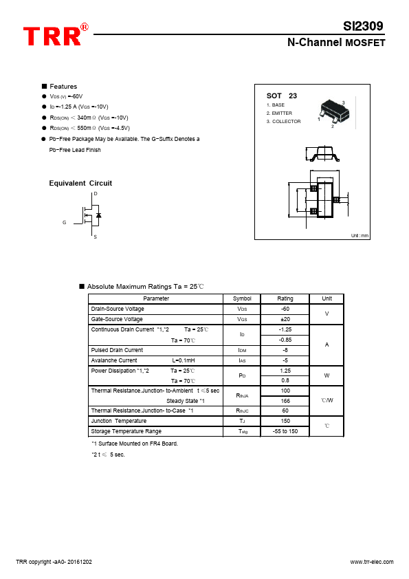
Equivalent Circuit
N-Channel MOSFET
SOT 23
1. BASE 2. EMITTER 3. COLLECTOR
Unit : mm
- Absolute Maximum Ratings Ta = 25℃
Parameter
Drain-Source Voltage
Gate-Source Voltage
Continuous Drain Current
- 1,- 2
Ta = 25℃
Ta = 70℃
Pulsed Drain Current
Avalanche Current
L=0.1m H
Power Dissipation
- 1,- 2
Ta = 25℃
Ta = 70℃
Thermal Resistance.Junction- to-Ambient t ≤5 sec
Steady State
- 1
Thermal Resistance.Junction- to-Case
- 1
Junction Temperature
Storage Temperature Range
- 1 Surface Mounted on FR4 Board.
- 2 t ≤ 5 sec.
Symbol VDS VGS
IDM IAS PD
Rth...