TSM2832 Description
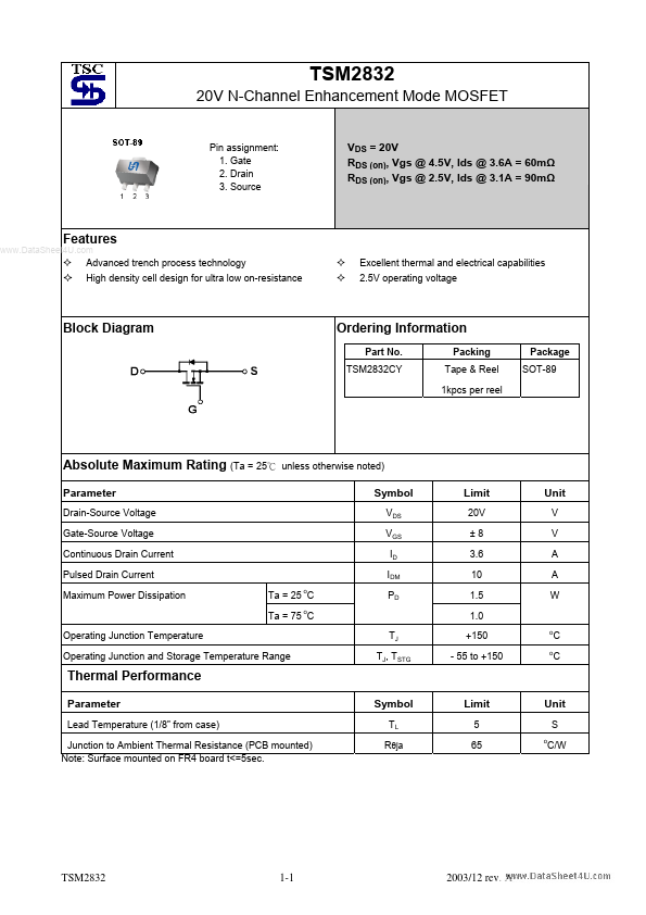
TSM2832 20V N-Channel Enhancement Mode MOSFET VDS = 20V RDS (on), Vgs @ 4.5V, Ids @ 3.6A = 60mΩ RDS (on), Vgs @ 2.5V, Ids @ 3.1A = 90mΩ Pin assignment:.
TSM2832 is 20V N-Channel Enhancement Mode MOSFET manufactured by Taiwan Semiconductor Company.
| Part Number | Description |
|---|---|
| TSM2831 | 20V P-Channel Enhancement Mode MOSFET |
| TSM2301 | 20V P-Channel Enhancement Mode MOSFET |
| TSM2301B | 20V P-Channel MOSFET |
| TSM2302 | 20V N-Channel Enhancement Mode MOSFET |
| TSM2306 | 30V N-Channel MOSFET |
TSM2832 20V N-Channel Enhancement Mode MOSFET VDS = 20V RDS (on), Vgs @ 4.5V, Ids @ 3.6A = 60mΩ RDS (on), Vgs @ 2.5V, Ids @ 3.1A = 90mΩ Pin assignment:.