2SK3131 Overview
Key Specifications
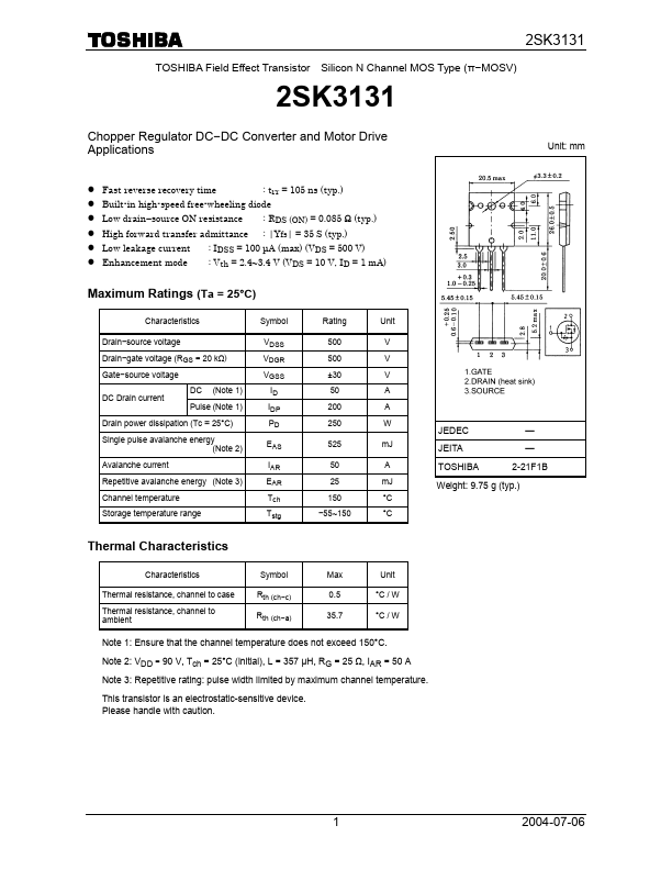
Mount Type: Through Hole
Pins: 3
Max Operating Temp: 150 °C
Min Operating Temp: -55 °C
Mount Type: Through Hole
Pins: 3
Max Operating Temp: 150 °C
Min Operating Temp: -55 °C
| Seller | Inventory | Price Breaks | Buy |
|---|---|---|---|
| Worldway Electronics | 11678 | 7+ : 1.2134 USD 10+ : 1.1891 USD 100+ : 1.1527 USD 500+ : 1.1163 USD |
View Offer |
| SHENGYU ELECTRONICS | 12055 | 1+ : 1.6845 USD 10+ : 1.6508 USD 100+ : 1.6 USD 1000+ : 1.55 USD |
View Offer |
| Part Number | Manufacturer | Description |
|---|---|---|
| 2SK3134L | Hitachi Semiconductor | N-Channel MOSFET |
| 2SK3136 | Hitachi Semiconductor | N-Channel MOSFET |
| 2SK3134 | Hitachi Semiconductor | N-Channel MOSFET |
| 2SK3134S | Hitachi Semiconductor | N-Channel MOSFET |
| 2SK3133 | Hitachi Semiconductor | N-Channel MOSFET |