2SK3132 Overview
Key Specifications
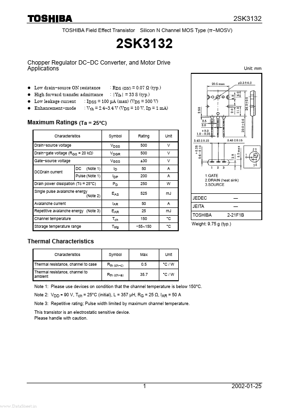
Mount Type: Through Hole
Pins: 3
Max Operating Temp: 150 °C
Min Operating Temp: -55 °C
Mount Type: Through Hole
Pins: 3
Max Operating Temp: 150 °C
Min Operating Temp: -55 °C
| Seller | Inventory | Price Breaks | Buy |
|---|---|---|---|
| Component Stockers USA | 623 | 1+ : 99.99 USD | View Offer |
| Win Source | 1300 | 1+ : 84.2907 USD 2+ : 69.1614 USD 3+ : 67.0004 USD 4+ : 64.8382 USD |
View Offer |
| Part Number | Manufacturer | Description |
|---|---|---|
| 2SK3134L | Hitachi Semiconductor | N-Channel MOSFET |
| 2SK3136 | Hitachi Semiconductor | N-Channel MOSFET |
| 2SK3134 | Hitachi Semiconductor | N-Channel MOSFET |
| 2SK3134S | Hitachi Semiconductor | N-Channel MOSFET |
| 2SK3133 | Hitachi Semiconductor | N-Channel MOSFET |