2SK3453
2SK3453 is N-Channel MOSFET manufactured by Toshiba.
..
TOSHIBA Field Effect Transistor Silicon N Channel MOS Type (π-MOSV)
Switching Regulator Applications
- -
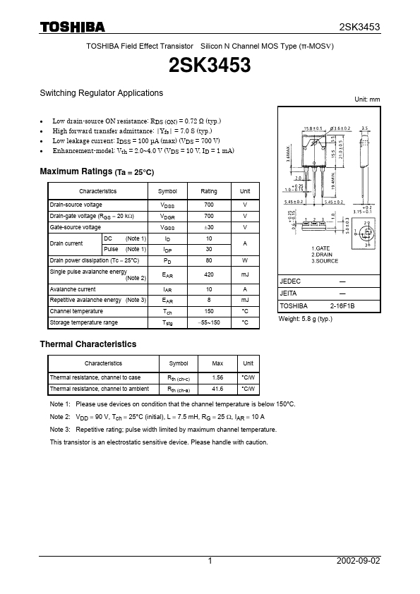
- - Low drain-source ON resistance: RDS (ON) = 0.72 Ω (typ.) High forward transfer admittance: |Yfs| = 7.0 S (typ.) Low leakage current: IDSS = 100 µA (max) (VDS = 700 V) Enhancement-model: Vth = 2.0~4.0 V (VDS = 10 V, ID = 1 m A) Unit: mm
Maximum Ratings (Ta = 25°C)
Characteristics Drain-source voltage Drain-gate voltage (RGS = 20 k W) Gate-source voltage Drain current DC Pulse (Note 1) (Note 1) Symbol VDSS VDGR VGSS ID IDP PD EAR IAR EAR Tch Tstg Rating 700 700 ±30 10 30 80 420 10 8 150 -55~150 Unit V V V A W m J A m J °C °C
Drain power dissipation (Tc = 25°C) Single pulse avalanche energy (Note 2) Avalanche current Repetitive avalanche energy (Note 3) Channel temperature Storage temperature range
JEDEC JEITA TOSHIBA
― ― 2-16F1B
Weight: 5.8 g (typ.)
Thermal Characteristics
Characteristics Thermal resistance, channel to case Thermal resistance, channel to ambient Symbol Rth (ch-c) Rth (ch-a) Max 1.56 41.6 Unit °C/W °C/W
Note 1: Please use devices on condition that the channel temperature is below 150°C. Note 2: VDD = 90 V, Tch = 25°C (initial), L = 7.5 m H, RG = 25 W, IAR = 10 A Note 3: Repetitive rating; pulse width limited by maximum channel temperature. This transistor is an electrostatic sensitive device. Please handle with caution.
2002-09-02
Electrical Characteristics (Ta = 25°C)
Characteristics Gate leakage current Drain-source breakdown voltage Drain cut-OFF current Drain-source breakdown voltage Gate threshold voltage Drain-source ON resistance Forward transfer admittance Input capacitance Reverse transfer capacitance Output capacitance Rise time Symbol IGSS V (BR) GSS IDSS V (BR) DSS Vth RDS (ON) ïYfsï Ciss Crss Coss tr VDS = 25 V, VGS = 0 V, f = 1 MHz Test Condition VGS = ±25 V, VDS = 0 V IG = ±10 m A, VDS = 0 V VDS = 700 V, VGS = 0 V ID = 10 m A, VGS = 0 V VDS = 10 V, ID = 1 m A VGS = 10 V, ID = 5 A VDS = 10 V, ID =...