2SK3667
2SK3667 is N-Channel MOSFET manufactured by Toshiba.
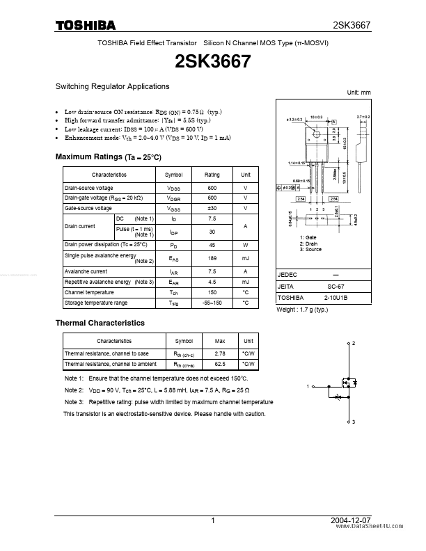
TOSHIBA Field Effect Transistor Silicon N Channel MOS Type (π-MOSVI)
Switching Regulator Applications
- -
- - Low drain-source ON resistance: RDS (ON) = 0.75Ω (typ.) High forward transfer admittance: |Yfs| = 5.5S (typ.) Low leakage current: IDSS = 100μA (VDS = 600 V) Enhancement mode: Vth = 2.0~4.0 V (VDS = 10 V, ID = 1 m A) Unit: mm
Maximum Ratings (Ta = 25°C)
Characteristics Drain-source voltage Drain-gate voltage (RGS = 20 kΩ) Gate-source voltage DC Drain current (Note 1) Symbol VDSS VDGR VGSS ID IDP PD EAS IAR EAR Tch Tstg Rating 600 600 ±30 7.5 30 45 189 7.5 4.5 150 -55~150 A W m J A m J °C °C
1: Gate 2: Drain 3: Source
Unit V V V
Pulse (t = 1 ms) (Note 1)
Drain power dissipation (Tc = 25°C) Single pulse avalanche energy (Note 2)
..
Avalanche current Repetitive avalanche energy (Note 3) Channel temperature Storage temperature range
JEDEC JEITA TOSHIBA
― SC-67 2-10U1B
Weight : 1.7 g (typ.)
Thermal Characteristics
Characteristics Thermal resistance, channel to case Thermal resistance, channel to ambient Symbol Rth (ch-c) Rth (ch-a) Max 2.78 62.5 Unit °C/W °C/W
Note 1: Ensure that the channel temperature does not exceed 150℃. Note 2: VDD = 90 V, Tch = 25°C, L = 5.88 m H, IAR = 7.5 A, RG = 25 Ω Note 3: Repetitive rating: pulse width limited by maximum channel temperature This transistor is an electrostatic-sensitive device. Please handle with caution.
3 1
2004-12-07
Electrical Characteristics (Ta = 25°C)
Characteristics Gate leakage current Gate-source breakdown voltage Drain cut-off current Drain-source breakdown voltage Gate threshold voltage Drain-source ON resistance Forward transfer admittance Input capacitance Reverse transfer capacitance Output capacitance Rise time Turn-on time Fall time Switching time Turn-off time Total gate charge Gate-source charge Gate-drain charge Symbol IGSS V (BR) GSS IDSS V (BR) DSS Vth RDS (ON) Test Condition VGS = ±25 V, VDS = 0 V IG =±10 µA, VDS = 0 V VDS = 600 V, VGS = 0 V ID = 10 m A, VGS...