SSM3J132TU
SSM3J132TU is Silicon P-Channel MOSFET manufactured by Toshiba.
MOSFETs Silicon P-Channel MOS (U-MOS- )
1. Applications
- Power Management Switches
2. Features
(1) 1.2-V drive (2) Low drain-source on-resistance
: RDS(ON) = 94 mΩ (max) (VGS = -1.2 V) RDS(ON) = 39 mΩ (max) (VGS = -1.5 V) RDS(ON) = 29 mΩ (max) (VGS = -1.8 V) RDS(ON) = 21 mΩ (max) (VGS = -2.5 V) RDS(ON) = 17 mΩ (max) (VGS = -4.5 V)
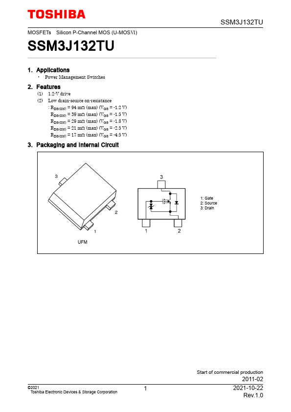
3. Packaging and Internal Circuit
1: Gate 2: Source 3: Drain
©2021
Toshiba Electronic Devices & Storage Corporation
Start of mercial production
2011-02
2021-10-22 Rev.1.0
4....