SSM3J13T
SSM3J13T is TOSHIBA Field Effect Transistor Silicon P Channel MOS Type manufactured by Toshiba.
TOSHIBA Field Effect Transistor Silicon P Channel MOS Type (U-MOSII)
Power Management Switch High Speed Switching Applications
- -
- Small Package Low on Resistance : Ron = 70 mΩ (max) (@VGS =
- 4 V) : Ron = 95 mΩ (max) (@VGS =
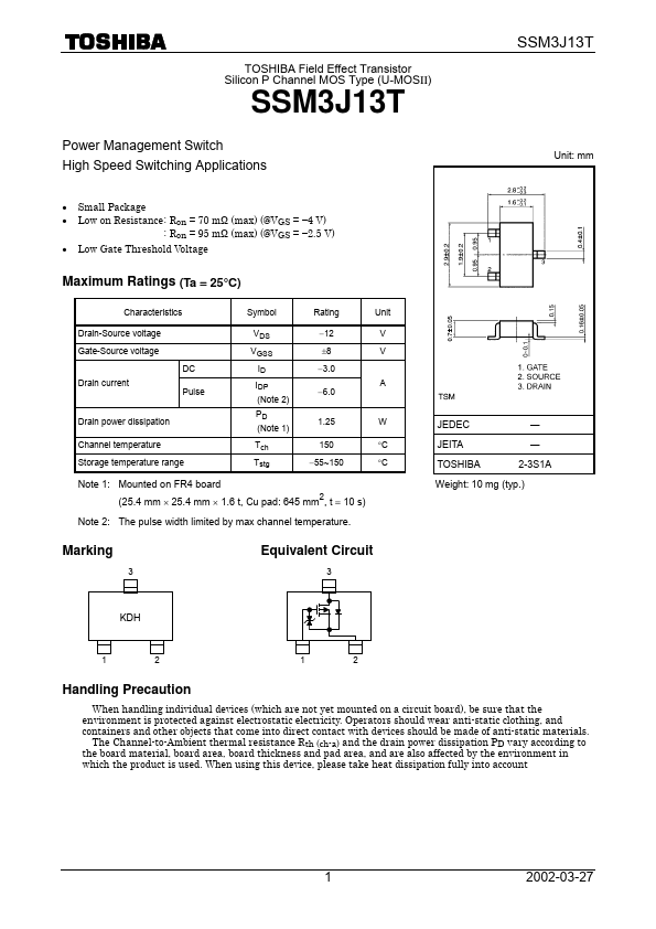
- 2.5 V) Low Gate Threshold Voltage Unit: mm
Maximum Ratings (Ta = 25°C)
Characteristics Drain-Source voltage Gate-Source voltage DC Drain current Pulse Symbol VDS VGSS ID IDP (Note 2) PD (Note 1) Tch Tstg Rating -12 ±8 -3.0 -6.0 1.25 150 -55~150 A Unit V V
Drain power dissipation Channel temperature Storage temperature range
W °C °C
JEDEC JEITA TOSHIBA
― ― 2-3S1A
Note 1: Mounted on FR4 board (25.4 mm ´ 25.4 mm ´ 1.6 t, Cu pad: 645 mm , t = 10...