SSM3J15F
SSM3J15F is Silicon P-Channel MOSFET manufactured by Toshiba.
TOSHIBA Field Effect Transistor Silicon P Channel MOS Type
High Speed Switching Applications Analog Switch Applications
- Small package
- Low ON resistance : Ron = 12 Ω (max) (@VGS =
- 4 V) : Ron = 32 Ω (max) (@VGS =
- 2.5 V)
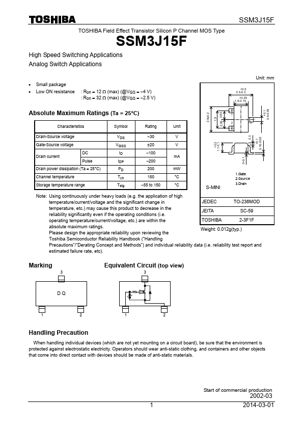
Unit: mm
+0.5 2.5-0.3
+0.25 1.5-0.15
+0.1 0.4-0.05
0.3 +0.1...