The following content is an automatically extracted verbatim text
from the original manufacturer datasheet and is provided for reference purposes only.
View original datasheet text
SSM3J15FV
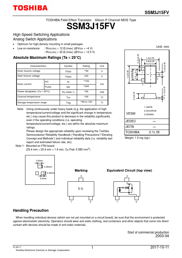
TOSHIBA Field Effect Transistor Silicon P Channel MOS Type
SSM3J15FV
High-Speed Switching Applications Analog Switch Applications
• Optimum for high-density mounting in small packages • Low on-resistance : RDS(ON) = 12 Ω (max) (@VGS = −4 V)
: RDS(ON) = 32 Ω (max) (@VGS = −2.5 V)
Absolute Maximum Ratings (Ta = 25°C)
Characteristics Drain-Source voltage Gate-Source voltage
Drain current
DC Pulse
Power dissipation (Ta = 25°C)
Channel temperature
Storage temperature range
Symbol
Rating
Unit
VDSS
−30
V
VGSS
±20
V
ID
−100
mA
IDP
−200
PD (Note 1)
150
mW
Tch
150
°C
Tstg
−55 to 150
°C
Note: Using continuously under heavy loads (e.g. the application of high temperature/current/voltage and the significant change in temperature, etc.