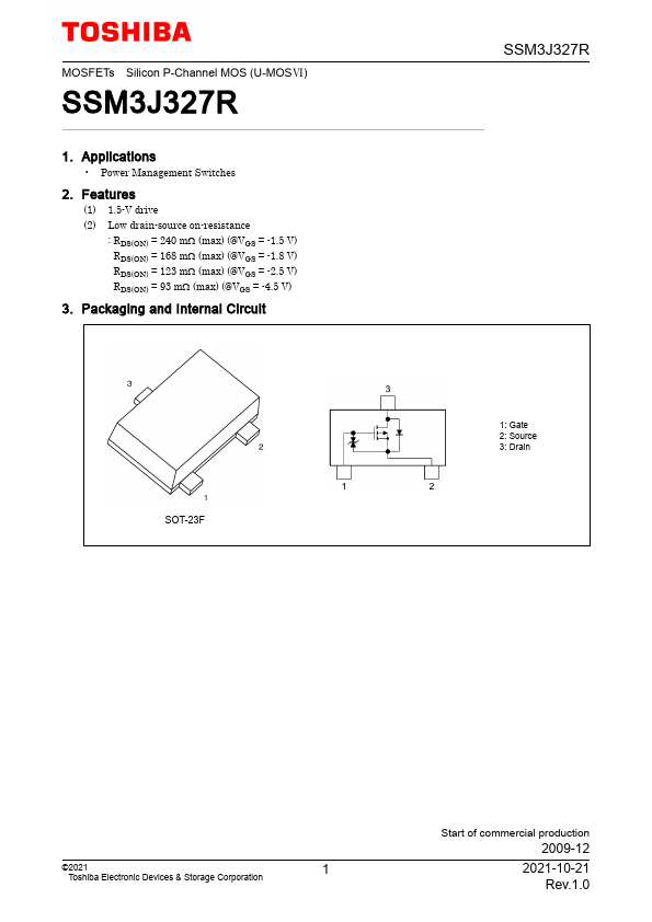
Datasheet4U Logo Datasheet4U.com

SSM3J327R - Silicon P-Channel MOSFET

Key Features

  • (1) 1.5-V drive (2) Low drain-source on-resistance : RDS(ON) = 240 mΩ (max) (@VGS = -1.5 V) RDS(ON) = 168 mΩ (max) (@VGS = -1.8 V) RDS(ON) = 123 mΩ (max) (@VGS = -2.5 V) RDS(ON) = 93 mΩ (max) (@VGS = -4.5 V) 3. Packaging and Internal Circuit SOT-23F SSM3J327R 1: Gate 2: Source 3: Drain ©2021 1 Toshiba Electronic Devices & Storage Corporation Start of commercial production 2009-12 2021-10-21 Rev.1.0 SSM3J327R 4. Absolute Maximum Ratings (Note) (Unless otherwise specified, Ta = 25.
  • ) C.

📥 Download Datasheet

Datasheet Details

Part number SSM3J327R
Manufacturer Toshiba
File Size 428.80 KB
Description Silicon P-Channel MOSFET
Datasheet download datasheet SSM3J327R Datasheet

Full PDF Text Transcription (Reference)

The following content is an automatically extracted verbatim text from the original manufacturer datasheet and is provided for reference purposes only.

View original datasheet text
MOSFETs Silicon P-Channel MOS (U-MOS�) SSM3J327R 1. Applications • Power Management Switches 2. Features (1) 1.5-V drive (2) Low drain-source on-resistance : RDS(ON) = 240 mΩ (max) (@VGS = -1.5 V) RDS(ON) = 168 mΩ (max) (@VGS = -1.8 V) RDS(ON) = 123 mΩ (max) (@VGS = -2.5 V) RDS(ON) = 93 mΩ (max) (@VGS = -4.5 V) 3. Packaging and Internal Circuit SOT-23F SSM3J327R 1: Gate 2: Source 3: Drain ©2021 1 Toshiba Electronic Devices & Storage Corporation Start of commercial production 2009-12 2021-10-21 Rev.1.0 SSM3J327R 4. Absolute Maximum Ratings (Note) (Unless otherwise specified, Ta = 25 �) Characteristics Symbol Rating Unit Drain-source voltage Gate-source voltage VDSS -20 V VGSS ±8 V Drain current (DC) (Note 1) ID -3.