Click to expand full text
MOSFETs Silicon P-Channel MOS (U-MOS�)
SSM6J503NU
1. Applications
• Power Management Switches
2. Features
(1) 1.5-V drive (2) Low drain-source on-resistance
: RDS(ON) = 89.6 mΩ (max) (@VGS = -1.5 V) RDS(ON) = 57.9 mΩ (max) (@VGS = -1.8 V) RDS(ON) = 41.7 mΩ (max) (@VGS = -2.5 V) RDS(ON) = 32.4 mΩ (max) (@VGS = -4.5 V)
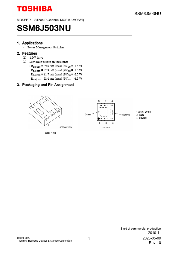
3. Packaging and Pin Assignment
UDFN6B
SSM6J503NU
1,2,5,6: Drain 3: Gate 4: Source
©2021-2025
1
Toshiba Electronic Devices & Storage Corporation
Start of commercial production
2010-11
2025-05-09 Rev.1.0
SSM6J503NU
4. Absolute Maximum Ratings (Note) (Unless otherwise specified, Ta = 25 �)
Characteristics
Symbol
Rating
Unit
Drain-source voltage Gate-source voltage
VDSS
-20
V
VGSS
±8
V
Drain current (DC)
(Note 1)
ID
-6.