SSM6K403TU
SSM6K403TU is Silicon N-Channel MOSFET manufactured by Toshiba.
MOSFETs Silicon N-Channel MOS
1. Applications
- Power Management Switches
- High-Speed Switching
2. Features
(1) 1.5-V drive (2) Low drain-source on-resistance
: RDS(ON) = 66 mΩ (max) (@VGS = 1.5 V) RDS(ON) = 43 mΩ (max) (@VGS = 1.8 V) RDS(ON) = 32 mΩ (max) (@VGS = 2.5 V) RDS(ON) = 28 mΩ (max) (@VGS = 4.0 V)
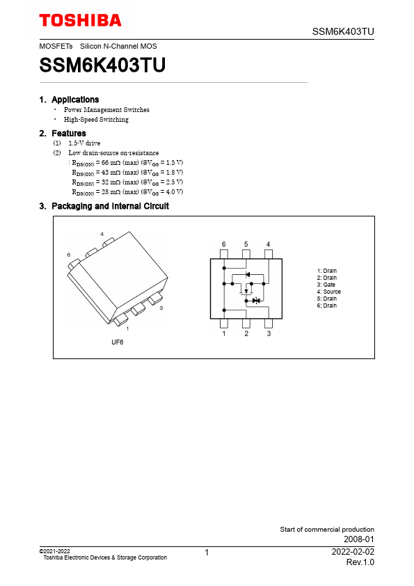
3. Packaging and Internal Circuit
UF6
1: Drain 2: Drain 3: Gate 4: Source 5: Drain 6; Drain
©2021-2022
Toshiba Electronic Devices & Storage Corporation
Start of mercial production
2008-01
2022-02-02 Rev.1.0
4....