TH58100FTI
TH58100FTI is TENTATIVE TOSHIBA MOS DIGITAL INTEGRATED CIRCUIT SILICON GATE CMOS manufactured by Toshiba.
TENTATIVE TOSHIBA MOS DIGITAL INTEGRATED CIRCUIT SILICON GATE CMOS
1-GBIT (128M × 8 BITS) CMOS NAND E PROM DESCRIPTION
The TH58100 is a single 3.3 V 1-Gbit (1,107,296,256) bit NAND Electrically Erasable and Programmable Read-Only Memory (NAND E2PROM) organized as 528 bytes × 32 pages × 8192 blocks. The device has a 528-byte static register which allows program and read data to be transferred between the register and the memory cell array in 528-byte increments. The Erase operation is implemented in a single block unit (16 Kbytes + 512 bytes: 528 bytes × 32 pages). The TH58100 is a serial-type memory device which utilizes the I/O pins for both address and data input/output as well as for mand inputs. The Erase and Program operations are automatically executed making the device most suitable for applications such as solid-state file storage, voice recording, image file memory for still cameras and other systems which require high-density non-volatile memory data storage.
Features
- Organization Memory cell allay 528 × 128K × 8 × 2 Register 528 × 8 Page size 528 bytes Block size (16K + 512) bytes Modes Read, Reset, Auto Page Program Auto Block Erase, Status Read Multi Block Program, Multi Block Erase Mode control Serial input/output mand control
- -
- - Power supply VCC = 2.7 V to 3.6 V Program/Erase Cycles 1E5 cycle (with ECC) Access time Cell array to register 25 µs max Serial Read Cycle 50 ns min Operating current Read (50 ns cycle) 10 m A typ. Program (avg.) 10 m A typ. Erase (avg.) 10 m A typ. Standby 100 µA Package TSOPI48-P-1220-0.50 (Weight: 0.53 g typ.)
- -
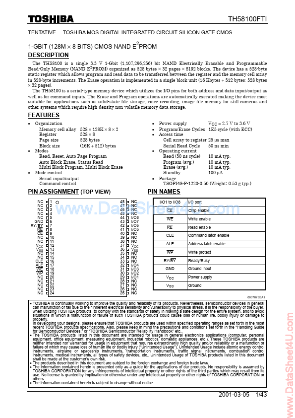
- PIN ASSIGNMENT (TOP VIEW)
NC NC NC NC NC GND
RE CE NC NC VCC VSS NC NC CLE ALE WE WP NC NC NC NC NC
PIN NAMES
48 47 46 45 44 43 42 41 40 39 38 37 36 35 34 33 32 31 30 29 28 27 26 25 NC NC NC NC I/O8 I/O7 I/O6 I/O5 NC NC NC VCC VSS NC NC NC I/O4 I/O3 I/O2 I/O1 NC NC NC NC I/O1 to I/O8
RY / BY
1 2 3 4 5 6 7 8 9 10 11 12 13 14 15 16 17 18 19 20 21 22 23...