TK40A10J1
TK40A10J1 is MOSFET manufactured by Toshiba.
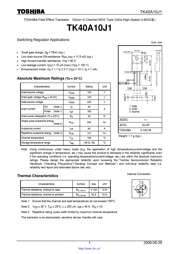
TOSHIBA Field Effect Transistor Silicon N Channel MOS Type (Ultra-High-Speed U-MOSⅢ)
Switching Regulator Applications
- -
- -
- Unit: mm Small gate charge: Qg = 76nC (typ.) Low drain-source ON-resistance: RDS (ON) = 11.5 mΩ (typ.) High forward transfer admittance: |Yfs| = 90 S Low leakage current: IDSS = 10 μA (max) (VDS = 100 V) Enhancement mode: Vth = 1.1 to 2.3 V (VDS = 10 V, ID = 1...