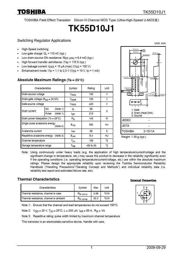
Datasheet Summary
TOSHIBA Field Effect Transistor Silicon N Channel MOS Type (Ultra-High-Speed U-MOSⅢ)
Switching Regulator Applications
- High-Speed switching
- Low gate charge: Qg = 110 nC (typ.)
- Low drain-source ON resistance: RDS (ON) = 8.4 mΩ (typ.)
- High forward transfer admittance: |Yfs| = 110 S (typ.)
- Low leakage current: IDSS = 10 μA (max) (VDS = 100 V)
- Enhancement mode: Vth = 1.1 to 2.3 V (VDS = 10 V, ID = 1...