TK70D06J1
TK70D06J1 is N-Channel MOSFET manufactured by Toshiba.
TOSHIBA Field Effect Transistor Silicon N Channel MOS Type (Ultra-High-Speed U-MOSⅢ)
Switching Regulator Application
- High-Speed switching
- Small gate charge: Qg = 87 n C (typ.)
- Low drain-source ON resistance: RDS (ON) = 5.1 mΩ (typ.)
- High forward transfer admittance: |Yfs| = 80 S (typ.)
- Low leakage current: IDSS = 10 μA (max) (VDS = 60 V)
- Enhancement-mode: Vth = 1.1 to 2.3 V (VDS = 10 V, ID = 1 m A)
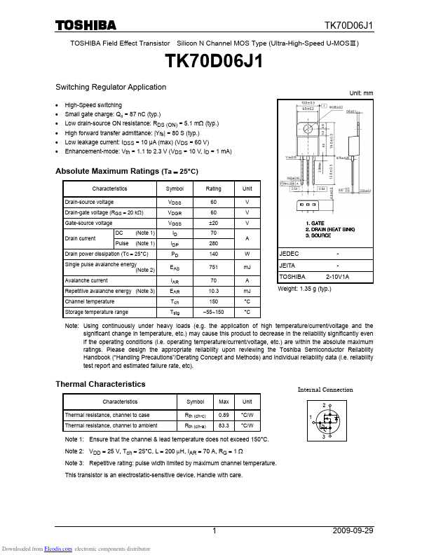
Unit: mm
Absolute Maximum Ratings (Ta = 25°C)
Characteristics
Symbol
Rating
Unit
Drain-source voltage
Drain-gate voltage (RGS = 20 kΩ) Gate-source voltage
Drain current
DC (Note 1) Pulse (Note 1)
Drain power dissipation (Tc = 25°C)
Single pulse avalanche energy (Note 2)
Avalanche current
Repetitive avalanche energy (Note 3)
Channel temperature
Storage temperature range
VDSS VDGR VGSS
ID IDP PD
IAR EAR Tch Tstg
60 60 ±20 70 280 140
70 10.3 150
- 55~150
W m J A m J °C °C
JEDEC
- JEITA
- TOSHIBA
2-10V1A
Weight: 1.35 g (typ.)
Note: Using continuously under heavy loads (e.g. the application of high temperature/current/voltage and the significant change in temperature, etc.) may cause this product to decrease in the reliability significantly even if the operating conditions (i.e. operating temperature/current/voltage, etc.) are within the absolute maximum ratings. Please design the appropriate reliability upon reviewing the Toshiba Semiconductor Reliability Handbook (“Handling Precautions”/Derating Concept and Methods) and individual reliability data (i.e. reliability test report and estimated failure rate,...