SSM6P56FE
SSM6P56FE is P-Channel MOSFET manufactured by Toshiba.
Features
(1) 1.2-V drive (2) Low drain-source on-resistance
: RDS(ON) = 390 mΩ (max) (@VGS = -4.5 V, ID = -800 m A) RDS(ON) = 480 mΩ (max) (@VGS = -2.5 V, ID = -500 m A) RDS(ON) = 660 mΩ (max) (@VGS = -1.8 V, ID = -200 m A) RDS(ON) = 900 mΩ (max) (@VGS = -1.5 V, ID = -100 m A) RDS(ON) = 4000 mΩ (max) (@VGS = -1.2 V, ID = -10 m A)
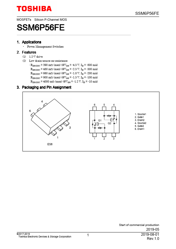
3. Packaging and Pin Assignment
ES6
1. Source1 2. Gate1 3. Drain2 4. Source2 5. Gate2 6. Drain1
©2017-2019 Toshiba Electronic Devices & Storage Corporation
Start of mercial production
2019-05
2019-08-01 Rev.1.0
4. Absolute Maximum Ratings (Note) (Unless otherwise specified, Ta = 25 ) (Q1,Q2 mon)
Characteristics
Symbol
Rating
Unit
Drain-source voltage Gate-source voltage Drain current (DC) Drain current (pulsed) Power dissipation Power dissipation
(Note 1) (Note 1) (Note 2) (Note 3)
VDSS VGSS
ID IDP PD
-20
±8
-800 m A
-1600
150 m W
Channel temperature Storage temperature
Tch
Tstg
-55 to 150
Note: Using continuously under heavy loads (e.g. the application of high temperature/current/voltage and the significant change in temperature, etc.) may cause this product to decrease in the reliability significantly even if the operating conditions (i.e. operating temperature/current/voltage, etc.) are within the absolute maximum ratings. Please design the appropriate reliability upon reviewing the Toshiba Semiconductor Reliability Handbook ("Handling Precautions"/"Derating Concept and Methods") and individual reliability data (i.e. reliability test report and estimated failure rate, etc).
Note 1: Ensure that the channel temperature does not exceed 150 . Note 2: Device mounted on an FR4 board.(total rating)
(25.4 mm × 25.4 mm × 1.6 mm, Cu pad: 0.135 mm2 × 6) Note 3: Device mounted on an FR4 board.(total rating)
(25.4 mm × 25.4 mm × 1.6 mm, Cu pad: 645 mm2)
Note:...