MAPLST2122-060CF
MAPLST2122-060CF is RF Power Field Effect Transistor manufactured by Tyco Electronics.
Features
Designed for W-CDMA base station applications in the 2.1 to 2.2 GHz Frequency Band. Suitable for TDMA, CDMA, and multicarrier power amplifier applications.
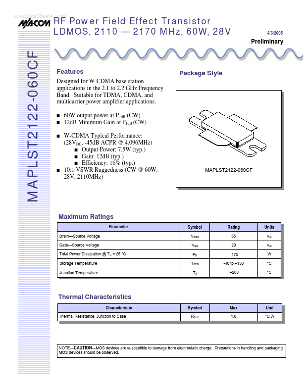
Package Style
60W output power at P1d B (CW) 12d B Minimum Gain at P1d B (CW) W-CDMA Typical Performance: (28VDC, -45d B ACPR @ 4.096MHz) Q Output Power: 7.5W (typ.) Q Gain: 12d B (typ.) Q Efficiency: 16% (typ.) 10:1 VSWR Ruggedness (CW @ 60W, 28V, 2110MHz)
Maximum Ratings
Parameter Drain- Source Voltage Gate- Source Voltage Total Power Dissipation @ TC = 25 °C Storage Temperature Junction Temperature Symbol VDSS VGS PD TSTG TJ Rating 65 20 175 -40 to +150 +200 Units Vdc Vdc W °C °C
Thermal Characteristics
Characteristic Thermal Resistance, Junction to Case Symbol RΘJC Max 1.0 Unit ºC/W
NOTE- CAUTION- MOS devices are susceptible to damage from electrostatic charge. Precautions in handling and packaging MOS devices should be observed.
RF Power LDMOS Transistor, 2110
- 2170 MHz, 60W, 28V
4/6/2005
Preliminary
Characteristic DC CHARACTERISTICS @ 25ºC Characteristic Drain-Source Breakdown Voltage (V GS = 0 Vdc, ID = 20 µAdc) OFF CHARACTERISTICS Zero Gate Voltage Drain Leakage Current (VDS 65 Vdc, VGS DS = 28 GS = 0) Gate- Source Leakage Zero Gate Voltage Drain Current Leakage Current (V Vdc, VV 0) DS = = (VGS = =5 26 Vdc, 0)
DS GS
Symbol
Min
Typ
Max
Unit
Symbol V(BR)DSS IDSS IDSS IGSS IDSS VGS(th) IGSS VDS(Q) VDS(on) Gm
Min 65
- -
- - 2
- 2
- -
Typ
- -
- -
- -
- - 0.4 2.4
Max
- 1 10 11 1 4
Unit Vdc µAdc µAdc µAdc µAdc Vdc µAdc Vdc Vdc S
Gate Threshold Voltage Gate- Source Leakage Current (VDS = 10 Vdc, ID = 1 m A) (VGS = 5 Vdc, VDS = 0) Gate Quiescent Voltage ON (V CHARACTERISTICS DS = 28 Vdc, ID = 500 m A) Drain-Source On-Voltage (VGS = 10 Vdc, ID = 1 A) Forward Transconductance (VGS = 10 Vdc, ID = 1 A) DYNAMIC CHARACTERISTICS @ 25ºC Input Capacitance (Including Input Matching DYNAMIC CHARACTERISTICS (1) Capacitor in Package) (VDS = 28 Vdc, VGS = 0, f = 1...