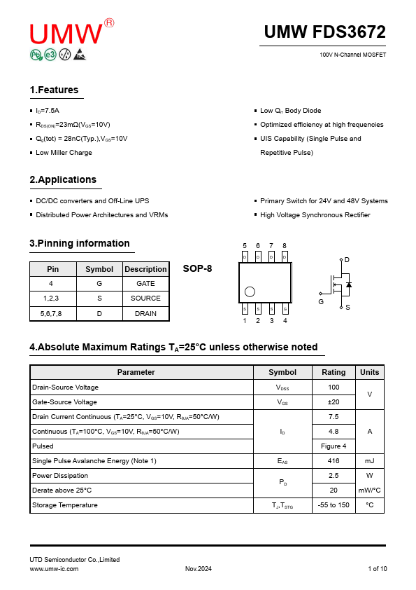
Datasheet4U Logo Datasheet4U.com

FDS3672 Datasheet 100v N-channei MOSFET

Manufacturer: UMW

Overview: UMW FDS3672 100V N-ChanneI MOSFET 1.

Datasheet Details

Part number FDS3672
Manufacturer UMW
File Size 1.54 MB
Description 100V N-ChanneI MOSFET
Datasheet FDS3672-UMW.pdf

General Description

GATE SOURCE DRAIN SOP-8 5678 D D D D S S S G 1234 D G S 4.Absolute Maximum Ratings TA=25°C unless otherwise noted Parameter Drain-Source Voltage Gate-Source Voltage Drain Current Continuous (TA=25°C, VGS=10V, RθJA=50°C/W) Continuous (TA=100°C, VGS=10V, RθJA=50°C/W) Pulsed Single Pulse Avalanche Energy (Note 1) Power Dissipation Derate above 25°C Storage Temperature Symbol VDSS VGS ID EAS PD TJ,TSTG Rating Units 100 V ±20 7.5 4.8 A Figure 4 416 mJ 2.5 W 20 mW/°C -55 to 150 °C UTD Semiconductor Co.,Limited www.umw-ic.com Nov.2024 1 of 10 www.umw-ic.com UMW FDS3672 100V N-ChanneI MOSFET 5.Thermal Characteristics Parameter Thermal Resistance, Junction to Ambient at 10 seconds (Note 3) Thermal Resistance, Junction to Ambient at 1000 seconds (Note 3) Thermal Resistance, Junction to Case (Note 2) Symbol RθJA RθJA RθJC Rating 50 85 25 Units °C/W °C/W °C/W 2 of 10 UTD Semiconductor Co.,Limited Nov.2024 www.umw-ic.com UMW FDS3672 100V N-ChanneI MOSFET 6.Electrical Characteristics (TJ=25°C unless otherwise noted) Parameter Off Characteristics Drain-Source Breakdown Voltage Zero Gate Voltage Drain Current Gate to Source Leakage Current On Characteristics Gate to Source Threshold Voltage Drain to Source On Resistance Dynamic Characteristics Input Capacitance Output Capacitance Reverse Transfer Capacitance Total Gate Charge at 10V Threshold Gate Charge Gate to Source Gate Charge Gate Charge Threshold to Plateau Gate to Drain “Miller” Charge Switching Characteristics (VGS=10V)

Key Features

  • ID=7.5A RDS(ON)=23mΩ(VGS=10V) Qg(tot) = 28nC(Typ. ),VGS=10V Low Miller Charge 2.

FDS3672 Distributor