The following content is an automatically extracted verbatim text
from the original manufacturer datasheet and is provided for reference purposes only.
View original datasheet text
UMW SI2319A
-40V P-ChanneI MOSFET
1.Features
VDS(V)=-40V RDS(ON)<70mΩ(VGS=10V), ID=-4.4A RDS(ON)<95mΩ(VGS=4.5V), ID=-3.5A
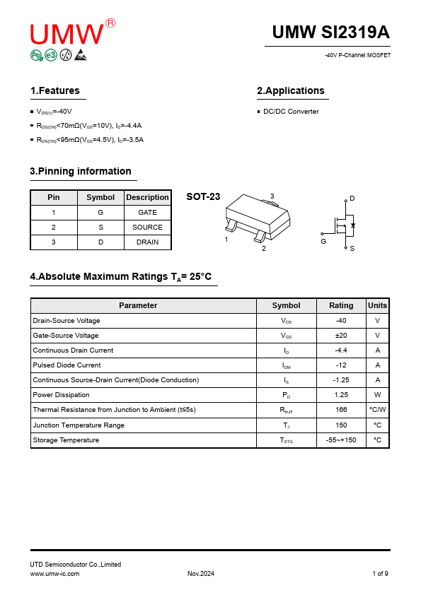
3.Pinning information
Pin
Symbol Description SOT-23
1
G
GATE
2
S
SOURCE
3
D
DRAIN
1
4.Absolute Maximum Ratings TA= 25°C
Parameter Drain-Source Voltage Gate-Source Voltage Continuous Drain Current Pulsed Diode Current Continuous Source-Drain Current(Diode Conduction) Power Dissipation Thermal Resistance from Junction to Ambient (t≤5s) Junction Temperature Range Storage Temperature
2.Applications
DC/DC Converter
3
D
G
2
S
Symbol VDS VGS ID IDM IS PD RthJF TJ TSTG
Rating -40 ±20 -4.4 -12 -1.25 1.25 166 150
-55~+150
Units V V A A A W
°C/W °C °C
UTD Semiconductor Co.,Limited www.umw-ic.com
Nov.2024
1 of 9
www.umw-ic.