CHA3511 Overview
Description
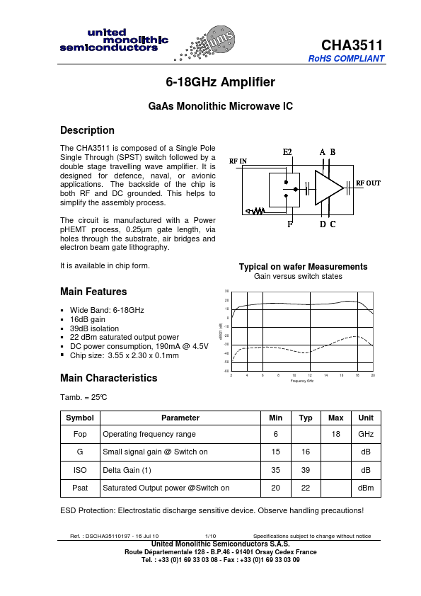
The CHA3511 is composed of a Single Pole Single Through (SPST) switch followed by a double stage travelling wave amplifier. It is designed for defence, naval, or avionic applications.
Key Features
- Observe handling precautions!
- Route Départementale 128 - B.P.46 - 91401 Orsay Cedex France Tel