CHA3512 Overview
Description
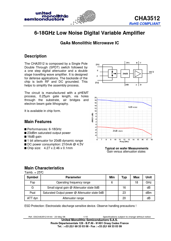
The CHA3512 is composed by a Single Pole Double Through (SPDT) switch followed by a one step digital attenuator and a double stage travelling wave amplifier. It is designed for defense applications.
Key Features
- Performances: 6-18GHz
- 23dBm saturated output power
- 1 bit attenuator for 20dB dynamic range
- DC power consumption: 210mA @ 4.5V