The following content is an automatically extracted verbatim text
from the original manufacturer datasheet and is provided for reference purposes only.
View original datasheet text
NDT451N-VB
PRODUCT SUMMARY
VDS (V) RDS(on) () at VGS = 10 V RDS(on) () at VGS = 4.5 V ID (A) Configuration
NDT451N-VB Datasheet N-Channel 30 V (D-S) MOSFET
30 0.019 0.021
7 Single
FEATURES • Trench Power MOSFET • 
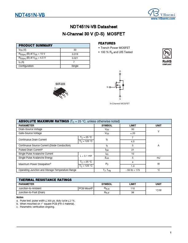
100 % Rg and UIS Tested
D
SOT-223 D
S D G
G
S N-Channel MOSFET
www.VBsemi.com
ABSOLUTE MAXIMUM RATINGS (TC = 25 °C, unless otherwise noted)
PARAMETER
SYMBOL
Drain-Source Voltage
VDS
Gate-Source Voltage
VGS
Continuous Drain Current
TC = 25 °C TC = 125 °C
ID
Continuous Source Current (Diode Conduction)
IS
Pulsed Drain Currenta
IDM
Single Pulse Avalanche Current Single Pulse Avalanche Energy
IAS L = 0.1 mH
EAS
Maximum Power Dissipationa
TC = 25 °C TC = 125 °C
PD
Operating Junction and Storage Temperature Range
TJ, Tstg
LIMIT 30 ± 20 7 4.5 5 31 10 5 4 1.