SIB406EDK
SIB406EDK is N-Channel MOSFET manufactured by Vishay.
FEATURES
- Halogen-free According to IEC 61249-2-21
- Trench FET® Power MOSFET
- New Thermally Enhanced Power PAK® SC-75 Package
- Small Footprint Area
- Low On-Resistance
- Typical ESD Protection 560 V
APPLICATIONS
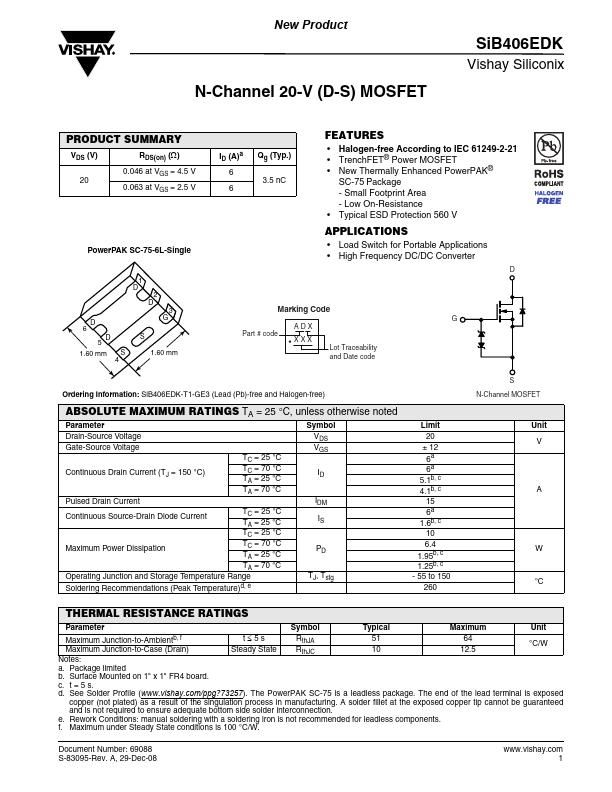
Power PAK SC-75-6L-Single
- Load Switch for Portable Applications
- High Frequency DC/DC Converter
1 D 2 D 3 6 D 5 D S 4 S 1.60 mm G ADX Part # code XXX Lot Traceability and Date code
Marking Code
1.60 mm
Ordering Information: Si B406EDK-T1-GE3 (Lead (Pb)-free and Halogen-free)
N-Channel MOSFET
ABSOLUTE MAXIMUM RATINGS TA = 25 °C, unless otherwise noted http://..net/
Parameter Drain-Source Voltage Gate-Source Voltage Continuous Drain Current (TJ = 150 °C) Pulsed Drain Current TC = 25 °C TA = 25 °C TC = 25 °C TC = 70 °C Maximum Power Dissipation TA = 25 °C TA = 70 °C Operating Junction and Storage Temperature Range Soldering Remendations (Peak Temperature)d, e Continuous Source-Drain Diode Current TC = 25 °C TC = 70 °C TA = 25 °C TA = 70 °C
Symbol VDS VGS ID IDM IS
PD TJ, Tstg
Limit 20 ± 12 6a 6a 5.1b, c 4.1b, c 15 6a 1.6b, c 10 6.4 1.95b, c 1.25b, c
- 55 to 150 260
Unit V
°C
THERMAL RESISTANCE RATINGS
Symbol Typical Maximum Unit t≤5s Rth JA 51 64 Maximum Junction-to-Ambientb, f °C/W Rth JC 10 12.5 Maximum Junction-to-Case (Drain) Steady State Notes: a. Package limited b. Surface Mounted on 1" x 1" FR4 board. c. t = 5 s. d. See Solder Profile (.vishay./ppg?73257). The Power PAK SC-75 is a leadless package. The end of the lead terminal is exposed copper (not plated) as a result of the singulation process in manufacturing. A solder fillet at the exposed copper tip cannot be guaranteed and is not required to ensure adequate bottom side solder interconnection. e. Rework Conditions: manual soldering with a soldering iron is not remended for leadless ponents. f. Maximum under Steady State conditions is 100 °C/W. Document Number: 69088 S-83095-Rev. A, 29-Dec-08 .vishay. 1 datasheet pdf
- http://..net/
Parameter
New Product
Si...