SUM110N06-3m4L
SUM110N06-3m4L is N-Channel MOSFET manufactured by Vishay.
FEATURES
- Trench FET® Power MOSFET
- 100 % Rg Tested
Ro HS
PLIANT
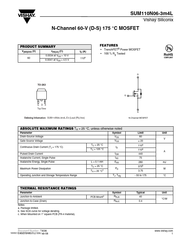
TO-263
Top View
Ordering Information: SUM110N06-3m4L-E3 (Lead (Pb)-free)
N-Channel MOSFET
ABSOLUTE MAXIMUM RATINGS TA = 25 °C, unless otherwise noted
Parameter Drain-Source Voltage Gate-Source Voltage Continuous Drain Current (TJ = 175 °C) Pulsed Drain Current Avalanche Current, Single Pulse Avalanche Energy, Single Pulse Maximum Power Dissipation Operating Junction and Storage Temperature Range L = 0.1 m H TC = 25 °C TA = 25 °Cc TC = 25 °C TC = 125 °C Symbol VDS VGS ID IDM IAS EAS PD TJ, Tstg Limit 60 ± 20 110a 110a 440 75 280 375b 3.75
- 55 to 175 m J W °C A Unit V
THERMAL RESISTANCE RATINGS
Parameter Junction-to-Ambient Junction-to-Case (Drain) Notes: a. Package limited. b. See SOA curve for voltage derating. c. When Mounted on 1" square PCB (FR-4 material). PCB Mountc Symbol Rth JA Rth JC Typical 40 0.4 Unit °C/W
Document Number: 73036 S-80272-Rev. B, 11-Feb-08
.vishay. 1
Vishay Siliconix
SPECIFICATIONS TJ = 25 °C, unless otherwise noted
Parameter Static Drain-Source Breakdown Voltage Gate Threshold Voltage Gate-Body Leakage Zero Gate Voltage Drain Current On-State Drain Currenta V(BR)DSS VGS(th) IGSS IDSS ID(on) VGS = 0 V, ID = 250 µA VDS = VGS, ID = 250 µA VDS = 0 V, VGS = ± 20 V VDS = 60 V, VGS = 0 V VDS = 60 V, VGS = 0 V, TJ = 125 °C VDS = 60 V, VGS = 0 V, TJ = 175 °C VDS ≥ 5 V, VGS = 10 V VGS = 10 V, ID = 30 A Drain-Source On-State Resistancea r DS(on) VGS = 4.5 V, ID = 20 A VGS = 10 V, ID = 30 A, TJ = 125 °C VGS = 10 V, ID = 30 A, TJ = 175 °C Forward Transconductancea Dynamicb Input Capacitance Output Capacitance Reverse Transfer Capacitance Total Gate Chargec Gate-Source Charge Gate-Drain Charge Gate Resistance Turn-On Delay Rise Timec Turn-Off Delay Timec Fall Timec c c
..
Symbol
Test Conditions
Min. 60 1
Typ.
Max.
Unit
3 ± 100 1 50 10
V n A µA m A A
120 0.0028 0.0033 0.0034 0.0041 0.0055 0.007 30 12900
Ω gfs Ciss Coss Crss Qg Qgs Qgd Rg td(on)...