Si4441EDY
Si4441EDY is P-Channel 30-V (D-S) MOSFET manufactured by Vishay.
FEATURES
- Trench FET® Power MOSFET
- ESD Protected: 2500 V
Pb-free Available
APPLICATIONS
- Battery and Load Switching
- Notebook
Ro HS-
PLIANT
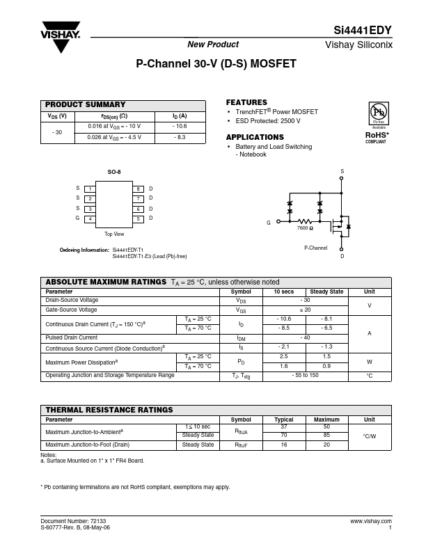
SO-8
S S S G 1 2 3 4 Top View Ordering Information: Si4441EDY-T1 Si4441EDY-T1-E3 (Lead (Pb)-free) P-Channel 8 7 6 5 D D D D G 7600
ABSOLUTE MAXIMUM RATINGS TA = 25 °C, unless otherwise noted
Parameter Drain-Source Voltage Gate-Source Voltage Continuous Drain Current (TJ = 150 °C)a Pulsed Drain Current Continuous Source Current (Diode Conduction)a Maximum Power Dissipationa Operating Junction and Storage Temperature Range TA = 25 °C TA = 70 °C TA = 25 °C TA = 70 °C Symbol VDS VGS ID IDM IS PD TJ, Tstg
- 2.1 2.5 1.6
- 55 to 150
- 10.6
- 8.5
- 40
- 1.3 1.5 0.9 W °C 10 secs Steady State
- 30 ± 20
- 8.1
- 6.5 A V Unit
THERMAL RESISTANCE RATINGS
Parameter Maximum Junction-to-Ambienta Maximum Junction-to-Foot (Drain) Notes: a. Surface Mounted on 1" x 1" FR4 Board. t ≤ 10 sec Steady State Steady State Symbol Rth JA Rth JF Typical 37 70 16 Maximum 50 85 20 Unit °C/W
- Pb containing terminations are not Ro HS pliant, exemptions may apply.
Document Number: 72133 S-60777-Rev. B, 08-May-06
.vishay. 1
Vishay Siliconix
New Product
SPECIFICATIONS TJ = 25 °C, unless otherwise noted
Parameter Static Gate Threshold Voltage Gate-Body Leakage Zero Gate Voltage Drain Current On-State Drain Currenta Drain-Source On-State Resistancea Forward Transconductancea Diode Forward Voltage Dynamicb Total Gate Charge Gate-Source Charge Gate-Drain Charge Turn-On Delay Time Rise Time Turn-Off Delay Time Fall Time Qg Qgs Qgd td(on) tr td(off) tf VDD =
- 15 V, RL = 15 Ω ID ≅
- 1 A, VGEN =
- 10 V, RG = 6 Ω VDS =
- 15 V, VGS =
- 10 V, ID =
- 10.6 A 45.5 6.5 12.5 5 11 45 35 8 20 70 55 ns 70 n C a
Symbol VGS(th) IGSS IDSS ID(on) r DS(on) gfs...