Si6993DQ
Si6993DQ is Dual P-Channel MOSFET manufactured by Vishay.
FEATURES
- Halogen-free
- Trench FET® Power MOSFETs
Ro HS
APPLICATIONS
- Load Switch
- Battery Switch
PLIANT
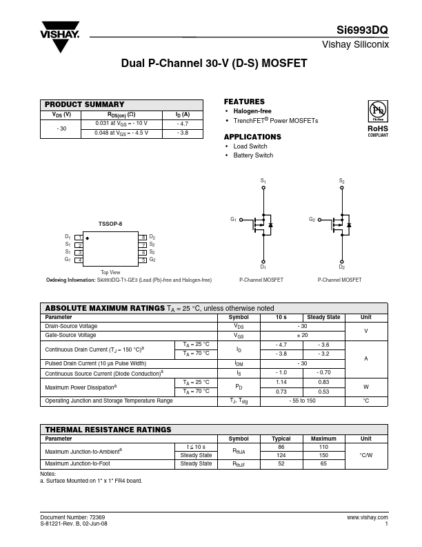
S1
S2
TSSOP-8
D1 S1 S1 G1 1 2 3 4 Top View Ordering Information: Si6993DQ-T1-GE3 (Lead (Pb)-free and Halogen-free) 8 D2 7 S2 6 S2 5 G2
G1
G2
D1 P-Channel MOSFET
D2 P-Channel MOSFET
ABSOLUTE MAXIMUM RATINGS TA = 25 °C, unless otherwise noted
Parameter Drain-Source Voltage Gate-Source Voltage Continuous Drain Current (TJ = 150 °C)a Pulsed Drain Current (10 µs Pulse Width) Continuous Source Current (Diode Conduction)a Maximum Power Dissipationa Operating Junction and Storage Temperature Range TA = 25 °C TA = 70 °C TA = 25 °C TA = 70 °C Symbol VDS VGS ID IDM IS PD TJ, Tstg
- 1.0 1.14 0.73
- 55 to 150
- 4.7
- 3.8
- 30
- 0.70 0.83 0.53 W °C 10 s Steady State
- 30 ± 20
- 3.6
- 3.2 A Unit V
THERMAL RESISTANCE RATINGS
Parameter Maximum Junction-to-Ambienta Maximum Junction-to-Foot Notes: a. Surface Mounted on 1" x 1" FR4 board. t ≤ 10 s Steady State Steady State Symbol Rth JA Rth JF Typical 86 124 52 Maximum 110 150 65 °C/W Unit
Document Number: 72369 S-81221-Rev. B, 02-Jun-08
.vishay. 1
Vishay Siliconix
SPECIFICATIONS TJ = 25 °C, unless otherwise noted
Parameter Static Gate Threshold Voltage Gate-Body Leakage Zero Gate Voltage Drain Current On-State Drain Currenta Drain-Source On-State Resistancea Forward Transconductancea Diode Forward Voltage Dynamicb Total Gate Charge Gate-Source Charge Gate-Drain Charge Gate Resistance Turn-On Delay Time Rise Time Turn-Off Delay Time Fall Time Source-Drain Reverse Recovery Time Qg Qgs Qgd Rg td(on) tr td(off) tf trr IF =
- 1.0 A, d I/dt = 100 A/µs VDD =
- 15 V, RL = 15 Ω ID ≅
- 1 A, VGEN =
- 10 V, RG = 6 Ω f = 1.0 MHz VDS =
- 15 V, VGS =
- 4.5 V, ID...