WFF9N50
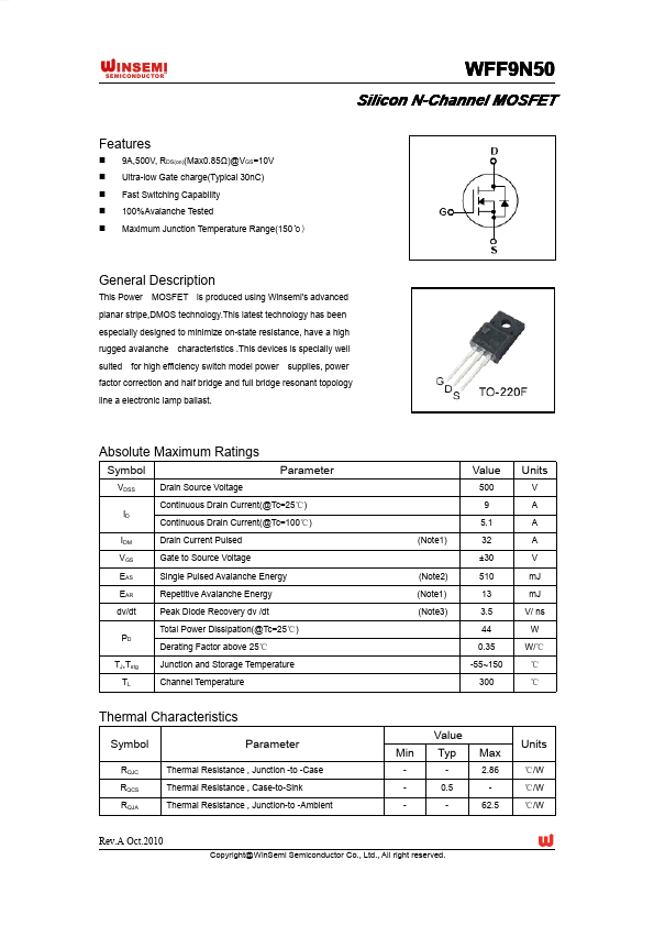
WFF9N50 is Silicon N-Channel MOSFET manufactured by WINSEMI SEMICONDUCTOR.
Features
- -
- -
- 9A,500V, RDS(on)(Max0.85Ω)@VGS=10V Ultra-low Gate charge(Typical 30n C) Fast Switching Capability 100%Avalanche Tested Maximum Junction Temperature Range(150℃)
General Description
This Power MOSFET is produced using Winsemi's advanced planar stripe,DMOS technology.This latest technology has been especially designed to minimize on-state resistance, have a high rugged avalanche characteristics .This devices is specially well suited for high efficiency switch model power supplies, power factor correction and half bridge and full bridge resonant topology line a electronic lamp ballast.
Absolute Maximum Ratings
Symbol
VDSS ID IDM VGS EAS EAR dv/dt PD TJ,Tstg TL Drain Source Voltage Continuous Drain Current(@Tc=25℃) Continuous Drain Current(@Tc=100℃) Drain Current Pulsed Gate to Source Voltage Single Pulsed Avalanche Energy Repetitive Avalanche Energy Peak Diode Recovery dv /dt Total Power Dissipation(@Tc=25℃) Derating Factor above 25℃ Junction and Storage Temperature Channel Temperature (Note2) (Note1) (Note3) (Note1)
Parameter
Value
500 9 5.1 32 ±30 510 13 3.5 44 0.35 -55~150 300
Units
V A A A V m J m J V/ ns W W/℃ ℃ ℃
Thermal Characteristics
Symbol
RQJC RQCS RQJA
Parameter
Thermal Resistance , Junction -to -Case Thermal Resistance , Case-to-Sink Thermal Resistance , Junction-to -Ambient
Value Min
- Typ
- Max
2.86 62.5
Units
℃/W ℃/W ℃/W
Rev.A Oct.2010
Copyright@Win Semi Semiconductor Co., Ltd., All right reserved.
.Data Sheet.in
Electrical Characteristics(Tc=25℃)
Characteristics
Gate leakage current Gate-source breakdown voltage
Symbol
IGSS V(BR)GSS
Test Condition
VGS=±30V,VDS=0V IG=±10 µA,VDS=0V VDS=500V,VGS=0V
Min
±30
- Type
-...