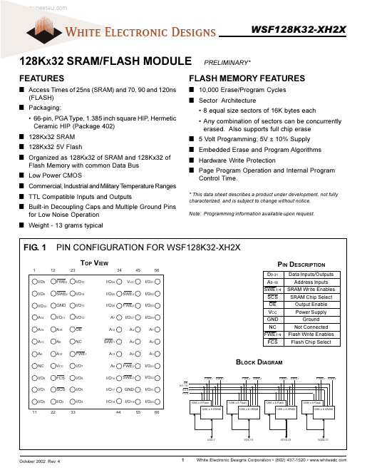
Datasheet Summary
..
White Electronic Designs
128KX32 SRAM/FLASH MODULE
Features
- Access Times of 25ns (SRAM) and 70, 90 and 120ns (FLASH)
- Packaging: 66-pin, PGA Type, 1.385 inch square HIP, Hermetic Ceramic HIP (Package 402)
- 128Kx32 SRAM
- 128Kx32 5V Flash
- Organized as 128Kx32 of SRAM and 128Kx32 of Flash Memory with mon Data Bus
- Low Power CMOS
- mercial, Industrial and Military Temperature Ranges
- TTL patible Inputs and Outputs
- Built-in Decoupling Caps and Multiple Ground Pins for Low Noise Operation
- Weight
- 13 grams typical PRELIMINARY-
FLASH MEMORY Features
- 10,000 Erase/Program Cycles
- Sector Architecture 8 equal size sectors of 16K bytes...