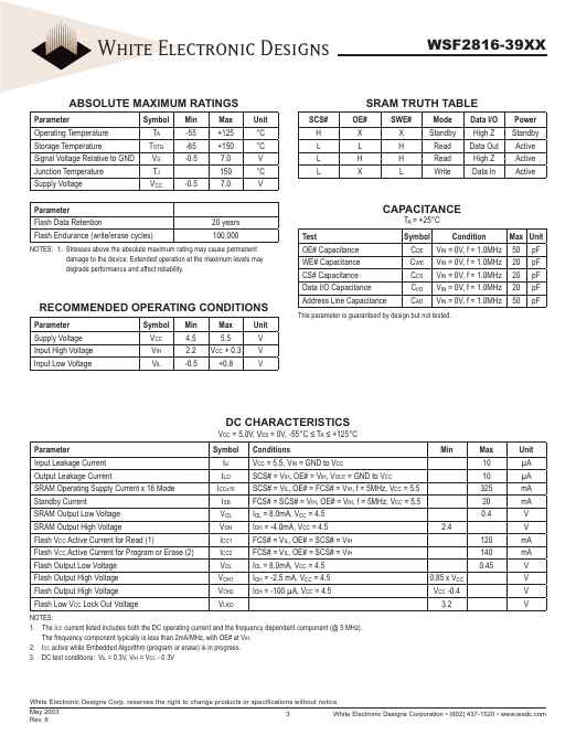
Datasheet Summary
..
White Electronic Designs
128KX16 SRAM/512KX16 FLASH MODULE
Features
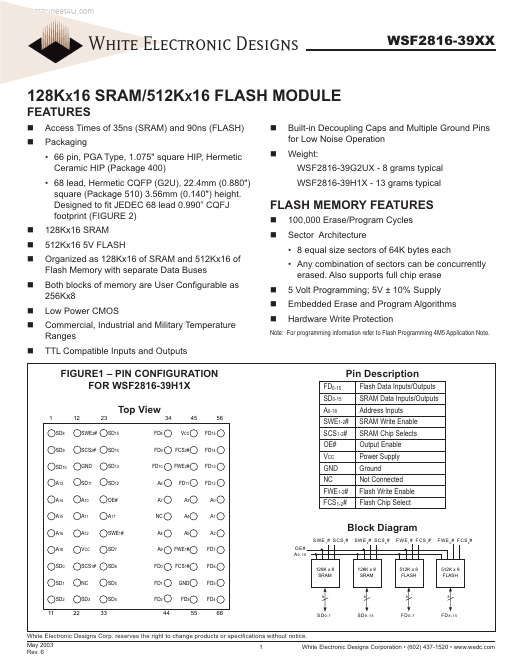
Access Times of 35ns (SRAM) and 90ns (FLASH) Packaging
- 66 pin, PGA Type, 1.075" square HIP, Hermetic Ceramic HIP (Package 400)
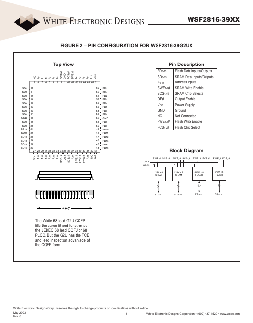
- 68 lead, Hermetic CQFP (G2U), 22.4mm (0.880") square (Package 510) 3.56mm (0.140") height. Designed to fit JEDEC 68 lead 0.990” CQFJ footprint (FIGURE 2) 128Kx16 SRAM 512Kx16 5V FLASH Organized as 128Kx16 of SRAM and 512Kx16 of Flash Memory with separate Data Buses Both blocks of memory are User Configurable as 256Kx8 Low Power CMOS mercial, Industrial and Military Temperature Ranges TTL patible Inputs and Outputs
Built-in Decoupling Caps and Multiple...