Datasheet Summary
..
White Electronic Designs
PRELIMINARY-
128KX32 SRAM & 512Kx32 FLASH MIXED MODULE
Features
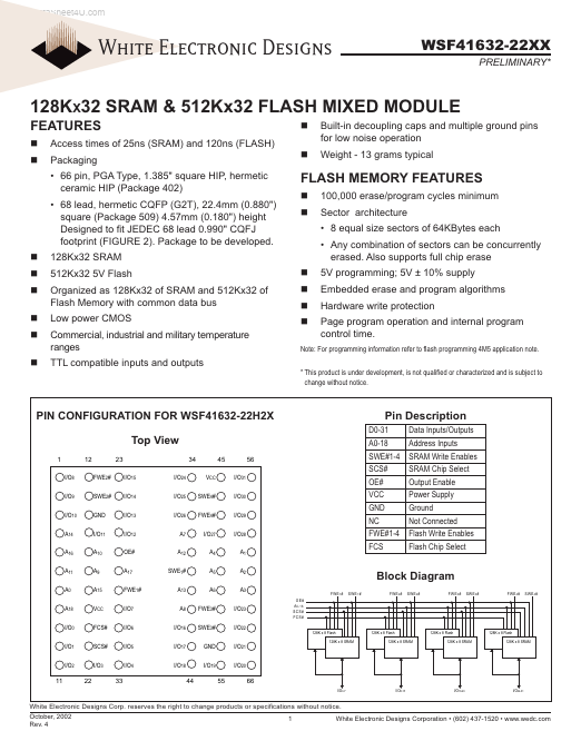
Access times of 25ns (SRAM) and 120ns (FLASH) Packaging
- 66 pin, PGA Type, 1.385" square HIP, hermetic ceramic HIP (Package 402)
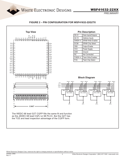
- 68 lead, hermetic CQFP (G2T), 22.4mm (0.880") square (Package 509) 4.57mm (0.180") height Designed to fit JEDEC 68 lead 0.990" CQFJ footprint (FIGURE 2). Package to be developed. 128Kx32 SRAM 512Kx32 5V Flash Organized as 128Kx32 of SRAM and 512Kx32 of Flash Memory with mon data bus Low power CMOS mercial, industrial and military temperature ranges TTL patible inputs and outputs
- This product is under development, is not...