WNM2021
WNM2021 is N-Channel MOSFET manufactured by Will Semiconductor.
Features z z z z z Trench Technology Supper high density cell design Excellent ON resistance Extremely Low Threshold Voltage Small package SOT-323
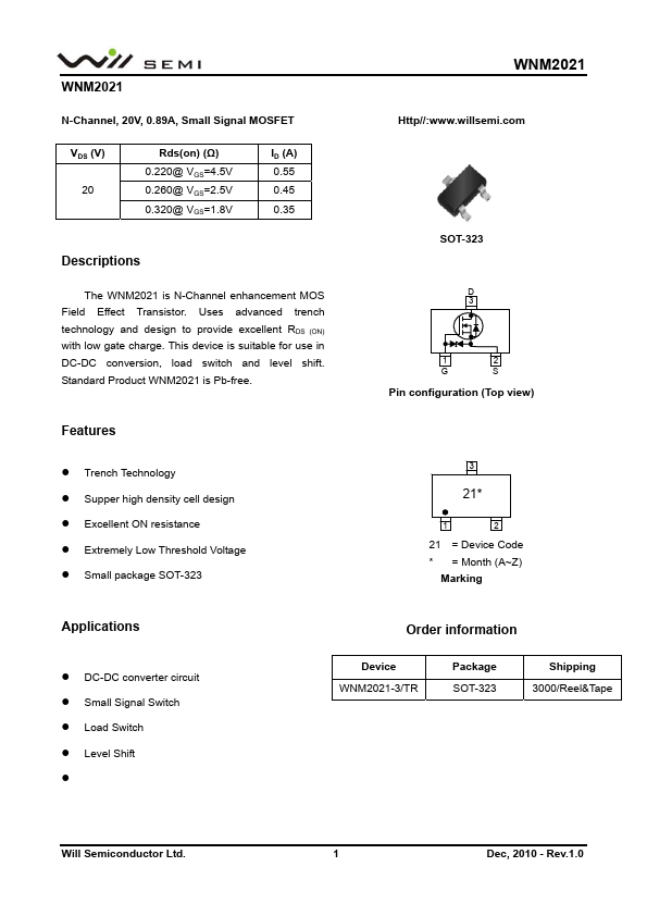
- 1 3
21-
21 = Device Code = Month (A~Z) Marking
Applications
Device
Order information
Package SOT-323 Shipping 3000/Reel&Tape z z z z z
DC-DC converter circuit Small Signal Switch Load Switch Level Shift
WNM2021-3/TR
Will Semiconductor Ltd.
Dec, 2010
- Rev.1.0
Absolute Maximum ratings
Parameter Drain-Source Voltage Gate-Source Voltage Continuous Drain Current a Maximum Power Dissipation a Continuous Drain Current b Maximum Power Dissipation b Pulsed Drain Current c Operating Junction Temperature Lead Temperature Storage Temperature Range TA=25°C TA=70°C TA=25°C TA=70°C TA=25°C TA=70°C TA=25°C TA=70°C Symbol VDS VGS ID PD ID PD IDM TJ TL Tstg 0.89 0.71 0.37 0.23 0.78 0.62 0.29 0.18 1.4 150 260
-55 to 150
10 S
Steady State 20 ±6 0.82 0.65 0.31 0.20 0.70 0.56 0.23 0.14
Unit V A W A W A °C °C °C
Thermal resistance ratings
Parameter Junction-to-Ambient Thermal Resistance a Junction-to-Ambient Thermal Resistance b Junction-to-Case Thermal Resistance t ≤ 10 s Steady State t ≤ 10 s Steady State Steady State Symbol RθJA RθJA RθJC Typical
275 325 375 445 260
Maximum
335 395 430 535 300
Unit
°C/W a b c d
Surface mounted on FR4 Board using 1 square inch pad size, 1oz copper Surface mounted on FR4 board using minimum pad size, 1oz copper Repetitive rating, pulse width limited by junction temperature, tp=10µs, Duty Cycle=1% Repetitive rating, pulse width limited by junction temperature TJ=150°C.
Will Semiconductor Ltd.
Dec, 2010
- Rev.1.0
Electronics Characteristics (Ta=25 C, unless otherwise noted) o
Parameter OFF CHARACTERISTICS Drain-to-Source Breakdown Voltage Zero Gate Voltage Drain Current Gate-to-source Leakage Current ON CHARACTERISTICS Gate Threshold Voltage Drain-to-source On-resistance
Symbol
Test Conditions
Min
Typ
Max...