SFTN3908MP
SFTN3908MP is N-Channel MOSFET manufactured by Winning Team.
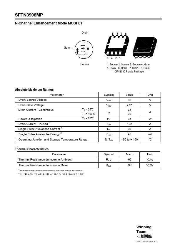
N-Channel Enhancement Mode MOSFET
Drain
Gate
Source
1. Source 2. Source 3. Source 4. Gate 5. Drain 6. Drain 7. Drain 8. Drain
DFN3030 Plastic Package
Absolute Maximum Ratings Parameter
Drain-Source Voltage
Drain-Gate Voltage Drain Current
- Continuous
Power Dissipation Drain Current
- Pulsed 1) Single Pulse Avalanche Current 2) Single Pulse Avalanche Energy 2)
TC = 25℃ TC = 100℃ TC = 25℃
Operating Junction and Storage Temperature Range
Thermal Characteristics Parameter
Thermal Resistance Junction to Ambient Thermal Resistance Junction to Case
1) Repetitive Rating : Pulsed width limited by maximum junction temperature. 2) VDD = 25 V, VGS = 10 V, L= 0.1m H, IAS = 30 A, RG = 25 Ω, Starting TJ = 25℃.
Symbol VDS VGS
PD IDM IAS EAS Tj, Tstg
Value 30 ± 20 48 30 35 192 30 45
- 55 to + 150
Symbol RθJA RθJC
Max. 62 3.6
Unit V V A W A A m J ℃
Unit ℃/W ℃/W
Winning Team 互創國際
Dated: 02/12/2017 PT
Characteristics at Tj = 25℃ unless otherwise specified
Parameter
Drain-Source Breakdown Voltage at ID = 250 µA
Gate-Source Threshold Voltage at VDS = VGS, ID = 250 µA
Drain-Source Leakage Current at VDS = 30 V at VDS = 24 V ,TJ = 125℃
Gate-Source Leakage Current at VGS = ± 20 V Drain-Source On-State Resistance at VGS = 10 V, ID = 16 A at VGS = 4.5 V, ID = 8 A Forward Transconductance at VDS = 10 V, ID = 8 A
Input Capacitance at VGS = 0 V, VDS = 25 V, f = 1 MHz
Output Capacitance at VGS = 0 V, VDS = 25 V, f = 1 MHz
Reverse Transfer Capacitance at VGS = 0 V, VDS = 25 V, f = 1 MHz
Turn-On Delay Time at VGS = 10 V, VDD = 15 V, ID = 15 A, RGEN = 3.3 Ω
Turn-On Rise Time at VGS = 10 V, VDD = 15 V, ID = 15 A, RGEN = 3.3 Ω
Turn-Off Delay Time at VGS = 10 V, VDD = 15 V, ID = 15 A, RGEN = 3.3...