XP6C036H
Description
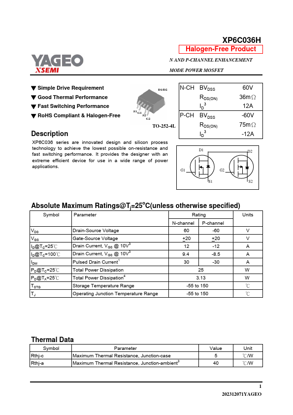
TO-252-4L
XP6C036 series are innovated design and silicon process technology to achieve the lowest possible on-resistance and fast switching performance. It provides the designer with an extreme efficient device for use in a wide range of power applications.
N-CH P-CH
G1
BVDSS RDS(ON) ID3 BVDSS RDS(ON) ID3
D1
G2
S1
60V 36mΩ
12A -60V 75mΩ -12A
D2
S2
Absolute Maximum Ratings@Tj=25o C(unless otherwise specified)
Symbol
Parameter
Rating
Units
N-channel P-channel
Drain-Source Voltage
-60
VGS ID@TC=25℃ ID@TC=100℃ IDM
Gate-Source Voltage Drain Current, VGS @ 10V3 Drain Current, VGS @ 10V3 Pulsed Drain Current1
+20
+20
-12
-8.5
-30
PD@TC=25℃ PD@TA=25℃
Total Power Dissipation Total Power Dissipation4
TSTG
Storage Temperature...