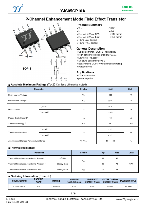
Datasheet Details
| Part number | YJS05GP10A |
|---|---|
| Manufacturer | Yangjie Electronic |
| File Size | 799.13 KB |
| Description | P-Channel Enhancement Mode Field Effect Transistor |
| Datasheet | YJS05GP10A-YangzhouYangjie.pdf |
|
|
|
Overview: YJS05GP10A RoHS PLIANT P-Channel Enhancement Mode Field Effect Transistor Product Summary ● VDS ● ID ● RDS(ON)( at VGS=-10V) ● RDS(ON)( at VGS=-4.5V) ● 100% EAS Tested ● 100% ▽VDS Tested -100V -4.
| Part number | YJS05GP10A |
|---|---|
| Manufacturer | Yangjie Electronic |
| File Size | 799.13 KB |
| Description | P-Channel Enhancement Mode Field Effect Transistor |
| Datasheet | YJS05GP10A-YangzhouYangjie.pdf |
|
|
|
● Split gate trench MOSFET technology ● High density cell design for low RDS(ON) ● Low Crss(Typ.25pF) ● Moisture Sensitivity Level 3 ● Epoxy Meets UL 94 V-0 Flammability Rating ● Halogen Free Applications ● DC motor control ● power supplies ■ Absolute Maximum Ratings (TA=25℃unless otherwise noted) Parameter Symbol Limit Unit Drain-source Voltage Gate-source Voltage Drain Current Pulsed Drain Current A Avalanche energy B TA=25℃ TA=100℃ VDS -100 V VGS ±20 V -4.5 ID A -2.85 IDM -18 A EAS 56 mJ Total Power Dissipation TA=25℃ TA=100℃ Junction and Storage Temperature Range PD TJ ,TSTG 1.65 W 0.65 -55~+150 ℃ ■Thermal resistance Parameter Thermal Resistance Junction-to-Ambient C Thermal Resistance Junction-to-Ambient C t≤10S Steady-State Symbol RθJA Typ Max Units 31 40 59 75 ℃/W Thermal Resistance Junction-to-Lead Steady-State RθJL 16 24 ■ Ordering Information (Example) PREFERED P/N PACKING CODE Marking YJS05GP10A F2 Q05P10A MINIMUM PACKAGE(pcs) 4000 INNER BOX QUANTITY(pcs) OUTER CARTON QUANTITY(pcs) DELIVERY MODE 8000 64000 13“ reel S-E433 Rev.1.2,30-Mar-23 1/6 Yangzhou Yangjie Electronic Technology Co., Ltd.
.21yangjie.
YJS05GP10A ■ Electrical Characteristics (TJ=25℃ unless otherwise noted) Parameter Symbol Conditions Min Typ Max Units Static Parameter Drain-Source Breakdown Voltage Zero Gate Voltage Drain Current Gate-Body Leakage Current Gate Threshold Voltage Static Drain-Source On-Resistance Diode Forward Voltage Maximum Body-Diode Continuous Current Dynamic Parameters BVDSS IDSS IGSS VGS(th) RDS(ON) VSD IS VGS= 0V, ID=-250μA VDS=-100V,VGS=0V TJ=25℃ TJ=150℃ VGS= ±20V, VDS=0V VDS= VGS, ID=-250μA VGS= -10V, ID=-3A VGS= -4.5V, ID=-2A IS=-3A
| Part Number | Description |
|---|---|
| YJS12G06A | N-Channel Enhancement Mode Field Effect Transistor |
| YJS12G06D | N-Channel Enhancement Mode Field Effect Transistor |
| YJS15G10B | N-Channel Enhancement Mode Field Effect Transistor |