ZXMN6A25DN8 Overview
Key Specifications
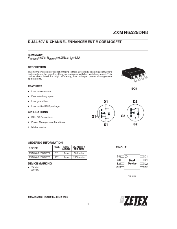
Package: SOIC
Mount Type: Surface Mount
Pins: 8
Height: 1.5 mm
Key Features
- Low on-resistance
- Fast switching speed
- Low gate drive
- Low profile SOIC package SO8
| Part | ZXMN6A25DN8 |
|---|---|
| Description | DUAL 60V N-CHANNEL MOSFET |
| Category | MOSFET |
| Manufacturer | Zetex Semiconductors |
| Size | 241.82 KB |
Package: SOIC
Mount Type: Surface Mount
Pins: 8
Height: 1.5 mm
| Seller | Inventory | Price Breaks | Buy |
|---|---|---|---|
| Future Electronics | 500 | 500+ : 0.725 USD 1000+ : 0.715 USD 1500+ : 0.71 USD 2000+ : 0.705 USD |
View Offer |
| Verical | 1500 | 176+ : 0.6775 USD | View Offer |
| Part Number | Manufacturer | Description |
|---|---|---|
| ZXMN6A25G | Diodes Incorporated | 60V SOT223 N-channel enhancement mode MOSFET |