Datasheet4U Logo Datasheet4U.com

CDC1104 - 1 to 4 Configurable Clock Buffer

General Description

The CDC1104 is a 1 to 4 configurable clock buffer.

The device accepts an input reference clock and creates 4 buffered output clocks with an output frequency equal to one half the input clock frequency.

Four control inputs, S1, S2, S3, S4 configurable phases of the clock outputs.

40°C to

Key Features

  • 1.
  • Input Reference Clock 120Hz.
  • 240Hz.
  • Output Clock (Fin/2) 60Hz.
  • 120Hz.
  • Output Buffer Drive Strength: 8mA.
  • 4 Clock Outputs.
  • 4 Control Pins Select Phases of Clock Outputs.
  • Supply Voltage: 3.8V.
  • 5.5V.
  • Operating Temperature Range:.
  • 40°C to 85°C.
  • ESD Protection Exceeds JESD 22.
  • 2000-V Human-Body Model (A114-B).
  • 500-V Charged-Device Model (C101).
  • Package Offerings.

📥 Download Datasheet

Full PDF Text Transcription (Reference)

The following content is an automatically extracted verbatim text from the original manufacturer datasheet and is provided for reference purposes only.

View original datasheet text
www.ti.com 1 to 4 Configurable Clock Buffer for 3D Displays Check for Samples: CDC1104 CDC1104 SCAS921 – SEPTEMBER 2011 FEATURES 1 • Input Reference Clock 120Hz–240Hz • Output Clock (Fin/2) 60Hz–120Hz • Output Buffer Drive Strength: 8mA • 4 Clock Outputs • 4 Control Pins Select Phases of Clock Outputs • Supply Voltage: 3.8V–5.5V • Operating Temperature Range: –40°C to 85°C • ESD Protection Exceeds JESD 22 – 2000-V Human-Body Model (A114-B) – 500-V Charged-Device Model (C101) • Package Offerings – 
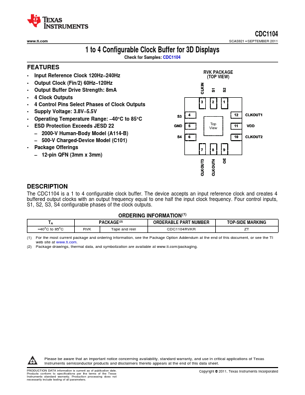
12-pin QFN (3mm x 3mm) RVK PACKAGE (TOP VIEW) CLKIN S1 S2 321 S3 4 GND 5 S4 6 Top View 12 CLKOUT1 11 VDD 10 CLKOUT2 789 CLKOUT3 CLKOUT4 OE DESCRIPTION The CDC1104 is a 1 to 4 configurable clock buffer.