Datasheet Summary
CDC111 1-LINE TO 9-LINE DIFFERENTIAL LVPECL CLOCK DRIVER
D Low-Output Skew for Clock-Distribution
Applications
D Differential Low-Voltage Pseudo-ECL
(LVPECL)-patible Inputs and Outputs
D Distributes Differential Clock Inputs to Nine
Differential Clock Outputs
D Output Reference Voltage, VREF , Allows
Distribution From a Single-Ended Clock Input
D Single-Ended LVPECL-patible Output
Enable
D Packaged in Plastic Chip Carrier description
SCAS321G
- SEPTEMBER 1993
- REVISED AUGUST 1999
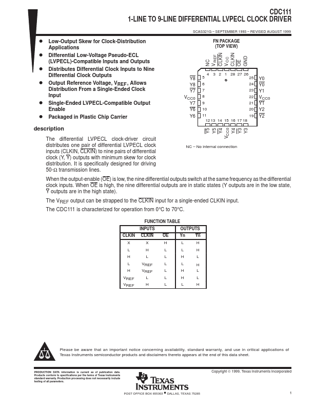
FN PACKAGE (TOP VIEW)
NC VREF CLKIN V CC CLKIN OE GND
Y8 Y8 Y7 VCC0 Y7 Y6 Y6
4 3 2 1 28 27 26 5 25 6 24 7 23 8 22 9 21 10 20 11 19
12 13 14 15 16 17 18
Y0 Y0 Y1 VCC0 Y1 Y2 Y2
Y5 Y5 Y4 VCC0 Y4 Y3...