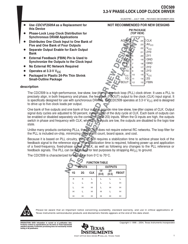
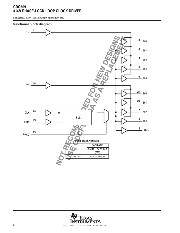
CDC509 Description
It uses a PLL to precisely align, in both frequency and phase, the feedback (FBOUT) output to the clock (CLK) input signal. It is specifically designed for use with synchronous DRAMs. The CDC509 operates at 3.3-V VCC and is designed to drive up to five clock loads per output.