CDCS503-Q1 Overview
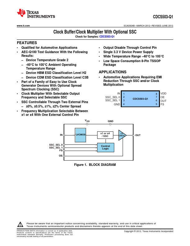
The CDCS503-Q1 device is a spread spectrum capable, LVCMOS input clock buffer with selectable frequency multiplication. It shares major functionality with the CDCS502 but uses a LVCMOS input stage instead of the crystal input stage of the CDCS502, and the CDCS503-Q1 has an output enable pin. The device accepts a 3.3-V LVCMOS signal at the input.
CDCS503-Q1 Key Features
- Qualified for Automotive
CDCS503-Q1 Applications
- AEC-Q100 Test Guidance With the Following