CDCS504-Q1 Description
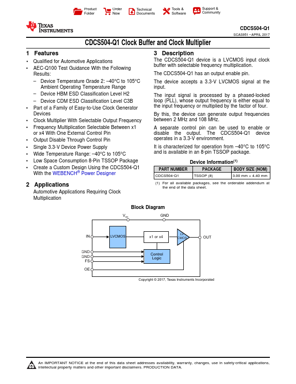
The CDCS504-Q1 device is a LVCMOS input clock buffer with selectable frequency multiplication. The CDCS504-Q1 has an output enable pin. The device accepts a 3.3-V LVCMOS signal at the input.
CDCS504-Q1 Key Features
- 1 Qualified for Automotive
CDCS504-Q1 Applications
- AEC-Q100 Test Guidance With the Following
- Device Temperature Grade 2: -40°C to 105°C