CDCS503 Overview
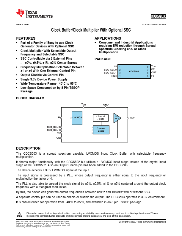
The CDCS503 is a spread spectrum capable, LVCMOS Input Clock Buffer with selectable frequency multiplication. It shares major functionality with the CDCS502 but utilizes a LVCMOS input stage instead of the crystal input stage of the CDCS502. Also an Output Enable pin has been added to the CDCS503.
CDCS503 Key Features
- Part of a Family of Easy to use Clock Generator Devices With Optional SSC
- Clock Multiplier With Selectable Output Frequency and Selectable SSC
- SSC Controllable via 2 External Pins
- ±0%, ±0.5%, ±1%, ±2% Center Spread
- Frequency Multiplication Selectable Between x1 or x4 With One External Control Pin
- Output Disable via Control Pin
- Single 3.3V Device Power Supply
- Wide Temperature Range -40°C to 85°C
- Low Space Consumption by 8 Pin TSSOP